Thin Film Deposition Technologies
Although “thin-film vapor deposition” may not sound terribly exciting it is one of the most important ways of making integrated circuits, and is also on its way to becoming one of the building blocks of nanotechnology. Basically, it involves applying a thin coating to another surface, usually by coaxing the coating material from a vaporous or dissolved state using electricity, high heat, chemical reactions, evaporation, or other techniques.
One of the most common (and oldest) types of thin-film deposition is electroplating. Here, the target object (such as a piece of jewelry) is immersed in a chemical bath that contains dissolved metal atoms (such as gold). An electric current applied between the target and the bath causes the atoms to deposit onto the target. Electroplating has been very widely used since the early 19th century to make plated silverware, chrome automobile bumpers, and thousands of other objects.
Another type of thin-film vapor deposition or electroplating is “sputtering.” Sputtering uses an electrode, usually heated to a temperature high enough to cause it to fling off hot atoms, which find their way to the “target” surface and form layers. Known since at least the early 1850s, Thomas Edison was apparently one of the first to use this process for a commercial product when he used it to apply a thin layer of metal to the outside of his wax phonograph recordings in 1904, in order to make metal molds of the recordings for mass-duplication. An important variation of sputtering is called “anodizing,” which is used to give aluminum automobile wheels and trim items a uniform, shiny surface. It’s also widely used on cookware to make it resistant to food sticking.
Beginning in the 1960s, researchers at Bell Telephone Laboratories used a new type of thin-film vapor deposition (which they called molecular beam epitaxy) to “grow” thin layers of a certain type of semiconductor material onto another type of semiconductor base, in order to create a sort of sandwich that could then be further processed to make transistors. In a special chamber, the coating material is heated to high heat, and then as atoms “boil” off, they are guided to the coated surface, where they form an extremely thin, crystalline layer.
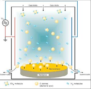
Today, thin-film deposition technology is capable of depositing layers of metals and other materials that are extremely thin and measured in mere nanometers. Both IBM and Hitachi, for example, use a process called chemical vapor deposition (CVD) to put magnetic coatings on computer hard discs. Most versions of the CVD process use hot gasses, often under pressure, and containing molecules or atoms of the coating material. This material is then deposited onto a surface through a chemical interaction between the gas and the surface. In the case of computer hard drives, CVD layers allow very large amounts of information to be stored on a small disc. Other researchers are using CVD to grow carbon nanotubes, as an alternative to other ways of making them. CVD manufacture is less costly than other methods, and many engineers anticipate that the reduction in cost in the first decade of the 21st century will make it economically viable to produce many more nanotube-based products. Because they are capable of producing nano-scale layers just a few atoms thick, CVD and similar techniques are sometimes called “nanotechology,” although some argue that the layer thickness alone does not constitute a true nanotechnology. However, it is true that thin-film manufacturing techniques are contributing to the first generation of true nanotechnologies, just as they have contributed to cutting-edge technology for over a century.
