Milestones:IBM Thomas J. Watson Research Center, 1960 - 1984
Citation
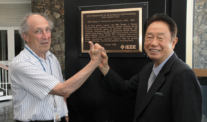
In its first quarter century, the IBM Thomas J. Watson Research Center produced numerous seminal advances having sustained worldwide impact in electrical engineering and computing. Semiconductor device innovations include dynamic random access memory (DRAM), superlattice crystals, and field effect transistor (FET) scaling laws. Computing innovations include reduced instruction set computer (RISC) architecture, integer programming, amorphous magnetic films for optical storage technology, and thin-film magnetic recording heads.
Street address(es) and GPS coordinates of the Milestone Plaque Sites
IBM Thomas J. Watson Research Center: 1101 Kitchawan Rd., Yorktown Heights, NY 10598 US (41.2098, -73.8026)
- See also the Visitor information page
Details of the physical location of the plaque
On one of the tall structural columns in the Main Lobby near the entrance
How the plaque site is protected/secured
- Visitors must request admission to see the plaque at least 48 hours in advance of a non-holiday weekday, and with an arrival time in the range of 8:30am-4pm (the site is open until 5pm). Do so by emailing your date/time request to IBM.YKT.IEEE.AWARD@ibm.com and receiving a confirmation.
- If arriving from Hwy 134/Kitchawan Rd, you will approach the front of the building. If arriving from Pinesbridge Rd, you will approach the rear of the building and will drive past the employee parking lot, heading toward the flagpole.
- Follow the signs toward the Visitor Parking Lot and drive to the "No Badge" security gate. Press the button and identify yourself to security, and you will be allowed to park. When you arrive at the Main Lobby, identify yourself as a visitor to see the Milestone plaque to receive a Visitors badge.
- Note that the Main Lobby also includes a Milestone plaque for the Semiconductor Laser and an American Physical Society plaque for the Watson Research Center.
Historical Significance
When IBM management decided to create a research organization that was independent of product development, the Watson Research Center was constructed as the headquarters for IBM Research. Throughout its first 25 years of operation, Watson Research Center employees have produced groundbreaking and enduring contributions to information technology, most notably through semiconductor device and computing innovations.
Seven of these achievements are especially noteworthy as watershed advances with sustained worldwide impact. Breakthrough innovations in semiconducting devices are dynamic random access memory (DRAM), superlattice crystals, and field effect transistor (FET) scaling laws. Breakthrough innovations in computing are reduced instruction set computer (RISC) architecture, integer programming, amorphous magnetic films for optical storage technology, and thin-film magnetic recording heads. No other corporate research institution has produced so many important advances in electrical engineering and computing that contributed to both the technical community and the business success of its parent corporation.
These seven technical achievements are detailed as follows:
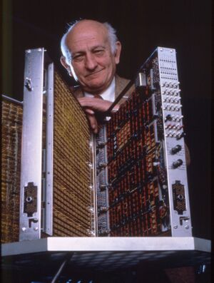
1. Semiconductor dynamic random access memory (DRAM) - the invention of the basic one-transistor dynamic memory cell used worldwide in virtually all modern computers. One-transistor DRAM became the standard of the industry for RAM and enabled the microcomputer revolution.
Major IEEE and other awards recognizing this achievement:
- 1982 IEEE Cledo Brunetti Award - Robert Dennard
- 1988 National Medal of Technology - Robert Dennard
- 1997 Inductee into the National Inventors Hall of Fame - Robert Dennard
- 2001 IEEE Edison Medal - Robert Dennard
- 2009 IEEE Medal of Honor – Robert Dennard
- 2009 NAE Draper Prize – Robert Dennard
Major reference documenting this achievement:
- US Patent 3,387,286, “Field-Effect Transistor Memory,” filed in 1967, issued in 1968
2. Semiconductor superlattice (multiple-quantum-well) crystals - the semiconductor superlattice is a man-made single-crystal with a periodic one-dimensional structural modification, produced by modulating either the alloy composition or impurity density during thin-film crystal growth. Such structures result in HEMT (high electron mobility transistor effect) transistors, high speed transistors now widely used in wireless telecommunications; room temperature, continuous wave, semiconductor lasers and photo-detectors now used in optical communications; and GMR (giant magnetoresistance) superlattice structures with very high sensitivity, now used for read heads in magnetic recording.
Major IEEE and other awards recognizing this achievement:
- 1985 APS Prize for New Materials – Leroy Chang, Leo Esaki, and Raphael Tsu
- 1991 IEEE Medal of Honor - Leo Esaki
Major references documenting this achievement:
- L. Esaki and R. Tsu, “Superlattice and Negative Differential Conductivity in Semiconductors,” IBM J. Res. Develop. 14, 61 (1970).
- US Patent 3,626,257, “Semiconductor Device with Superlattice Region,” filed in 1969, issued in 1971
- L. Esaki and L. L. Chang, “New Transport Phenomenon in a Semiconductor ‘Superlattice’,” Phys. Rev. Letters 33, 495 (1974)
3. Field effect transistor (FET) scaling laws - a concept of reducing the dimensions of metal-oxide field effect transistors (MOSFETs) and their interconnecting wires, leading to simultaneous improvements in transistor density, switching speed and power dissipation. This theory was presented in the seminal paper published in the IEEE Journal of Solid State Circuits in 1974. It is now a “Classic Paper” as recognized by the Proceedings of the IEEE, vol. 87, April 1999. The scaling theory has driven miniaturization in the semiconductor industry by giving the industry a roadmap, a method for setting targets and expectations for coming generations of process technology. This roadmap has been followed for over three decades, enabling computing to be portable, from laptops to cell phones to other technological devices.
Major IEEE and other awards recognizing this achievement:
- 1982 IEEE Cledo Brunetti Award - Robert Dennard
- 1988 National Medal of Technology - Robert Dennard
- 2001 IEEE Edison Medal - Robert Dennard
- 2009 IEEE Medal of Honor – Robert Dennard
- 2009 NAE Draper Prize – Robert Dennard
Major references documenting this achievement:
- R. H. Dennard, F. H. Gaensslen, H-N Yu, V. L. Rideout, E. Bassour, and A. R. LeBlanc, “Design of Ion-Implanted MOSFET’s with Very Small Physical Dimensions,” IEEE J. Solid-State Circuits SC-9, 256 (Oct. 1974)
- D. L. Critchlow, “MOSFET Scaling – The Driver of VLSI Technology,“ Proc. IEEE 87, 659 (April 1999) (Electronic file: IEEE Proc 1999_Critchlow_FET scaling.pdf)
4. Reduced Instruction Set Computer (RISC) architecture - development and implementation of a computer architecture that significantly increased the speed and efficiency of computers.
RISC architecture represents a central processing unit (CPU) design strategy emphasizing the insight that simplified instructions, which "do less", may still provide for higher performance if this simplicity can be utilized to make instructions execute very quickly. When first conceived, the RISC concept was contrary to the established direction of the functionally more complex instruction set computer (CISC) architecture. RISC was a fundamentally new concept in system design. Today, RISC microprocessors serve as the engines of most large, powerful computers.
In the 1960s and 1970s, instruction sets for computers became more and more complex. In addition to frequently executed primitive instructions, such as add, multiply, shift, etc., computer designers added many extremely complex instructions thought to be necessary for the programmers and for the compilers of the time. These complex instructions were relatively costly in that they required many more circuits and more machine time to execute them. In the mid 1970s, IBM Watson Researchers developed RISC architecture from a detailed study of the trade-offs between high performance machine organization and compiler optimization technology. An appropriately defined set of machine instructions, program controls, and programs produced by a compiler -- carefully designed to exploit the instruction set -- could realize a very high performance processor with relatively few circuits. RISC architecture enabled computers to run twice as fast on the same number of circuits.
Major IEEE and other awards recognizing this achievement:
- 1985 IEEE Computer Society Eckert-Mauchly Award - John Cocke
- 1987 ACM Turing Award - John Cocke
- 1989 IEEE Computer Society Pioneer Award - John Cocke
- 1991 National Medal of Technology - John Cocke
- 1994 IEEE John von Neumann Medal - John Cocke
- 1994 National Medal of Science - John Cocke
- 1999 IEEE Computer Society Seymour Cray Computer Sci. & Eng. Award -John Cocke
Major references documenting this achievement:
- John Cocke, “The Search for Performance in Scientific Processors,” Turing Acceptance Speech, Comm. ACM 31, 250 (March 1988)
- John Cocke and V. Markstein, “The evolution of RISC technology at IBM,” IBM J. Res. Develop. 34, 4 (1990)
5. Integer Programming and Discrete Optimization - creation of a general theory of integer programming and its application to particular problems in discrete optimization.
Integer programming is used for discrete optimation problems, e.g. airline scheduling, inventory management, military logistics and strategy, cutting stock or paper and similar commodities to fill orders with minimal waste. Mathematical work of this nature has been of major importance to the information procession industry. Because its sources were the realistic problems of manufacturing, transportation, and many other fields of commerce, engineering, and economics, the results were quickly useful and were aimed at economic pay-off.
Integer programming and discrete optimization was one of the first of the sciences in which large scale computation clearly led the way from the beginning. Techniques were developed at IBM Watson for solving certain classes of very large linear programming problems that had been believed to be intractable because of their enormous size. These techniques are now used in dealing with mixed integer – non integer problems, and provide many of the standard techniques used by optimizers.
Major IEEE and other awards recognizing this achievement:
- 1984 IEEE Computer Soc. Harry H. Goode Memorial Award - Ralph Gomory
- 1984 John von Neumann Theory Prize of INFORMS - Ralph Gomory
- 1988 National Medal of Science – Ralph Gomory
- 1994 IEEE Honorary Member - Ralph Gomory
Major references documenting this achievement:
- P. C. Gilmore and R. E. Gomory, “A Linear Programming Approach to the Cutting-Stock Problem,” Operations. Res. 9, 849 (1961)
- P. C. Gilmore and R. E. Gomory, “The Theory and Computation of Knapsack Functions,” Operations. Res. 14, 1045 (1966)
- Ralph E. Gomory, “Some Polyhedra Related to Combinatorial Problems,” Linear Algebra and Its Applications 2, 451 (1969)
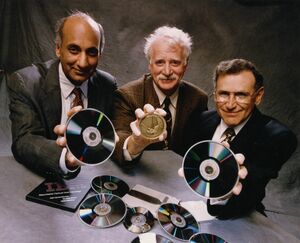
6. Amorphous Magnetic Films for Optical Storage Technology - discovery and development of amorphous magnetic materials, the basis of erasable, read-write, optical storage technology, now the foundation of the worldwide magneto-optic disk industry.
These magnetic materials, paradoxically, have built-in uniaxial magnetic anisotropy, despite being amorphous. Such materials, in thin-film form, are ideal as the magneto-optic storage materials for read/write optical storage systems.
In 1973, IBM Watson scientists published two papers on Amorphous Metallic Films, reporting magnetic anisotropy in thin films of GdCo alloy. These papers identified a major new materials system, as well as a series of fundamental properties of great interest and possible applications. Additional studies were carried out at IBM Research in the 1970s and early 1980s on the basic magnetic structure, the anisotropy, the magnetic coercivity, and the electronic properties of these materials.
These discoveries, studies, and publications laid the foundation for the now flourishing industry of erasable, read-write optical storage media. Optical storage systems are now an important area in the computer industry. Many companies world-wide produce optical storage systems (e.g., CD R/W, DVD R/W) based on these materials, making it a multi-billion dollar industry.
Major IEEE and other awards recognizing this achievement:
- 1992 IEEE Morris N. Liebmann Memorial Award – Praveen Chaudhari, Jerome Cuomo, and Richard Gambino
- 1995 National Medal of Technology - Praveen Chaudhari, Jerome Cuomo, and Richard Gambino
Major references documenting this achievement:
- P. Chaudhari, J.J. Cuomo, and R.J. Gambino, “Amorphous metallic films for magneto-optic applications,” Appl. Phys. Letters 22, 337 (1973)
- US Patent 3,949,387, “Beam Addressable Film using Amorphous Magnetic Material,” filed in 1972, issued in 1976
7. Thin-Film Magnetic Recording Heads - innovations in thin-film fabrication processes to realize inductive and magnetoresistive thin-film heads for large scale magnetic storage, significantly increasing the storage density of magnetic recording, and making rapid data access and storage possible on the Internet.
Since the commercial introduction of the first thin film heads in 1979, magnetic storage bit density has increased by 5 orders of magnitude. Without this capability to store and access, at tremendous speeds, an enormous amount of data on magnetic disk drives, many technologies we now take for granted would not exist, such as desktop and laptop computers, access to enormous libraries of data in fractions of seconds, modern banking systems and automatic teller machines, and, in particular, the Internet.
Since the introduction of IBM’s first magnetic disk storage system in 1956, the density of storage and speed of access has continuously improved. A quantum jump in the rate of improvement was enabled by the invention of thin film, read/write magnetic recording heads by scientists at the IBM Watson. They invented entirely new and unique fabrication processes, new designs of both read and write heads, and developed a new concept of mass fabrication of three dimensional objects of magnetic head structures on planar surfaces. These processes produce read/write heads consisting of three dimensional, high aspect ratio structures of magnetic yokes and tightly packed copper coils, with an entire cross section area small than that of a human hair. These inventions permitted the shrinking of the disk size from 12 inches to 1 inch in diameter and the shrinkage of the size of the entire storage device from room-size to credit card-size.
The total Direct Access Storage Device (DASD) industry revenue, dependent on thin-film magnetic recording heads, is ~$50 Billion/year and, despite the continuous drop in the price of devices, is growing.
Major IEEE and other awards recognizing this achievement:
- 1984 Electrochemical Society Electrodeposition Division Research Award – Lubomyr Romankiw and Robert J. von Gutfeld
- 1992 IEEE Cledo Brunetti Award – David Thompson
- 1994 IEEE Morris N. Liebmann Memorial Award – Lubomyr Romankiw
Major references documenting this achievement:
- US Patent 3,908,194, “Integrated Magnetoresistive Read, Inductive Write, Batch Fabricated Magnetic Head,” filed in 1974, issued in 1975
- US Patent 4,295,173, “Thin Film Inductive Transducer,” filed in 1979, issued in 1981 *L. T. Romankiw, “Electrodeposited Magnetic Thin Film Heads: A Quantum Jump for Magnetic Recording; Immense Impact on Development of Electrochemical Technology,” Plenary Address at 8th International Symposium on Magnetic Materials, Process and Devices, during 206th Meeting of The Electrochemical Society (October 2004) (Published as IBM Research Report RC24133, March 20, 1006)
Significant references


