Milestones:Semiconductor Laser, 1962
- Date Dedicated
- 2024/02/02
- Dedication #
- 247
- Location
- Niskayuna, NY
- Yorktown Heights, NY
- Lexington, MA
- IEEE Regions
- 1
- IEEE sections
- Schenectady, New York, Boston
- Achievement date range
- 1962


Title
Semiconductor Laser, 1962
Citation
In the autumn of 1962, General Electric’s Schenectady and Syracuse facilities, IBM Thomas J. Watson Research Center, and MIT Lincoln Laboratory each independently reported the first demonstrations of the semiconductor laser. Smaller than a grain of rice, powered using direct current injection, and available at wavelengths spanning the ultraviolet to the infrared, the semiconductor laser became ubiquitous in modern communications, data storage, and precision measurement systems.
Street address(es) and GPS coordinates of the Milestone Plaque Sites
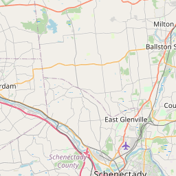
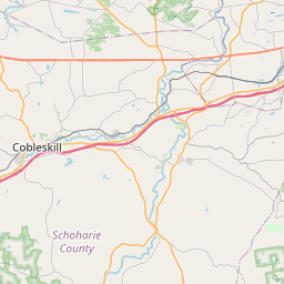
- Site 1: GE Global Research, 1 Research Circle, Niskayuna, NY 12309 US (42.8312, -73.8797)
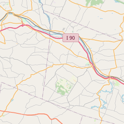
- Site 2: IBM Thomas J. Watson Research Center: 1101 Kitchawan Rd., Yorktown Heights, NY 10598 US (41.2098, -73.8026)
- Site 3: MIT Lincoln Laboratory: 244 Wood St., Lexington, MA 02421 US (42.458626, -71.263568)
- Site entrance gate is on Wood St. at Schilling Circle
- Plaque location: Main Lobby (42.45913, -71.26700)
Details of the physical location of the plaque
- Site 1: K West B Level, North: Mounted on the wall near the semiconductor research laboratories
- Site 2: On one of the tall structural columns in the Main Lobby near the entrance
- Site 3: One of 6 Milestone plaques on a display board prominently located in the Main Lobby
How the plaque site is protected/secured
- Site 1: Security gate; visitors must be registered and approved before entering, and must have a GE employee chaperone at all times. Gain access through Todd Alhart at 518.338.5880
- Site 2:
- Visitors must request admission to see the plaque at least 48 hours in advance of a non-holiday weekday, and with an arrival time in the range of 8:30am-4pm (the site is open until 5pm). Do so by emailing your date/time request to IBM.YKT.IEEE.AWARD@ibm.com and receiving a confirmation.
- If arriving from Hwy 134/Kitchawan Rd, you will approach the front of the building. If arriving from Pinesbridge Rd, you will approach the rear of the building and will drive past the employee parking lot, heading toward the flagpole.
- Follow the signs toward the Visitor Parking Lot and drive to the "No Badge" security gate. Press the button and identify yourself to security, and you will be allowed to park. When you arrive at the Main Lobby, identify yourself as a visitor to see the Milestone plaque to receive a Visitors badge.
- Note that the Main Lobby also includes two plaques honoring the Watson Research Center: an IEEE Milestone plaque and an American Physical Society plaque.
- Site 3: Building security is next to the display board; viewable during normal business hours
Historical significance of the work
Sixty years after its invention, the semiconductor laser has become a foundational element in a vast range of human endeavors, including optical communications (e.g., transcontinental undersea fiber-optic cables, data-center interconnects, free-space links connecting ground, air, and space), data storage and retrieval (e.g., compact disks [CDs] and digital video disks [DVDs]), human-machine interactions (e.g., computer-mouse pointing devices, laser pointers, printers, and light displays), manufacturing (e.g., industrial cutting and welding), medicine (e.g., optical coherence tomography [OCT]), and even in our leisure activities in the form of children’s toys and displays. Perhaps nowhere else has the semiconductor laser had greater impact than in communications, where every second, a semiconductor laser quietly encodes the sum of human knowledge into light, enabling it to be shared almost instantaneously across oceans and space. This capability is possible at tremendous scale and economy because the semiconductor laser realizes all the elements of a laser – light generation and amplification, lenses, and mirrors – within a solid microminiature block of material.
The enabling characteristics of the semiconductor laser include its small size (i.e., typically less than a cubic millimeter), its efficiency at converting electrical energy into coherent laser light, and its availability in a wide range of colors (or wavelengths) across the spectrum from ultraviolet (UV) to long-wave infrared (LWIR) to terahertz (THz). These desirable attributes attracted the imagination of scientists and engineers who, through decades of innovation, transformed the initial comparatively feeble semiconductor laser into the society-underpinning technology it is today. Still, the semiconductor laser’s potential is not fully tapped, as it is continually used to explore and exploit the realm of quantum mechanics in the service of mankind.
Obstacles (technical, political, geographic) that needed to be overcome
The realization of the semiconductor laser required decades of collaboration between theorists, mathematicians, materials scientists, engineers, and technicians. At the time the theoretical quantum mechanics underpinning the semiconductor laser was set down in the early twentieth century, very little of the materials science knowledge required to make the semiconductor laser existed. This situation changed rapidly after the invention of the semiconductor transistor in 1948.
Spurred by the semiconductor transistor’s success, several corporate and government laboratories had at hand the fertile mix of minds and technology necessary to realize the semiconductor laser. When it was reported at professional society meetings in summer 1962 that nearly 100% of the electrical energy injected into a gallium arsenide semiconductor could be converted into light, several research groups were poised to translate this knowledge into a working semiconductor laser. Within the span of roughly one month in fall 1962, the first semiconductor lasers were independently demonstrated at four research institutions. Following these seminal demonstrations, the concept was quickly replicated and expanded upon in research laboratories worldwide.
Features that set this work apart from similar achievements
In the few years between the demonstrations of the first laser (1960) and the semiconductor laser (1962), lasers could only be realized by an assembly of multiple discrete components, including an optical gain medium (e.g., doped glasses and crystals, atomic and molecular gases) that generated and amplified the light, a “pump” mechanism that energized the gain medium (e.g., flash lamp, electric discharge), and optical elements (e.g., mirrors, waveguides) that guided light and created a resonant cavity. In contrast, semiconductor materials could convert electrical energy directly into light, realizing both functionalities of the gain medium and pump in a single component. Moreover, the additional structures required to create a laser – optics for guiding the light and mirrors for the formation of a resonant cavity – could also be realized within the semiconductor material.
Because all this functionality came together in a tiny volume (less than 1 mm<sup>3</sup>), it could be economically produced in high volume. And in contrast to preceding laser technologies that were limited to fixed discrete colors (or wavelengths), the alloys making up the semiconductor material could be continuously varied in composition to create a wide range of laser colors, allowing the semiconductor laser to address many different applications within the same fundamental structure.
Significant references
[1] R. N. Hall, G. E. Fenner, J. D. Kingsley, T. J. Soltys, and R. O. Carlson, “Coherent light emission from GaAs junctions,” Phys. Rev. Lett., v. 9, p. 366, 1962. Media:Hall_CoherentLightEmissionFromGaAsJunctions_PhysRevLett9p366_1962.pdf
[2] M. I. Nathan, W. P. Dumke, G. Burns, F. H. Dill, Jr., and G. Lasher, “Stimulated emission of radiation from GaAs p-n junctions,” Appl. Phys. Lett., v. 1, p. 62, 1962. Media: Nathan_StimulatedLightEmissionfFromGaAsJunctions_APL1p62_1962.pdf
[3] N. Holonyak, Jr., and S. F. Bevacqua, “Coherent (visible) light emission from Ga(As1-xPx) junctions,” Appl. Phys. Lett., v. 1, p. 82, 1962. Media: Holonyak_CoherentVisibleLightEmissionFromGaAsPJunctions_APL1p82_1962.pdf
[4] T. M. Quist, R. H. Rediker, R. J. Keyes, W. E. Krag, B. Lax, A. L. McWhorter, H. J. Zeigler, “Semiconductor maser of GaAs,“ Appl. Phys. Lett, v. 1, p. 91, 1962. Media: Quist_SemiconductorMASERofGaAs_APL1p91_1962.pdf
[5] “Two Concerns Make Same Discovery,” The New York Times, November 1, 1962. Media:NYT_semiconductor_laser_article_621101.pdf
[6] R.N. Hall, "Injection Lasers," IEEE JOURNAL OF QUANTUM ELECTRONICS, VOL. QE-23. NO. 6, June1987. Media:Hall_InjectionLasers_JQE23p674_1987.pdf
[7] M.I. Nathan, "Invention of the Injection Laser at IBM," IEEE JOURNAL OF QUANTUM ELECTRONICS, VOL. QE-23, NO. 6, JUNE 1987.Media:Nathan_Invention_of_the_injection_laser_at_IBM_JQE23p679_1987.pdf
[8] N. Holonyak, "Semiconductor Alloy Lasers - 1962," IEEE JOURNAL OF QUANTUM ELECTRONICS, VOL. QE-23. NO. 6, JUNE 1987. Media:Holonyak_SemiconductorAlloyLasers_JQE23p684_1987.pdf
[9] R.H. Redicker, "Research at Lincoln Laboratory Leading upto the Development of the Injection Laser in 1962," IEEE JOURNAL OF QUANTUM ELECTRONICS. VOL. QE-21. NO. 6, JUNE 1987. Media:Rediker_Research_at_Lincoln_laboratory_leading_up_to_the_development_of_the_injection_laser_in_1962_JQE23p692_1987.pdf
Supporting materials
- IEEE Spectrum story: Inside the Three-Way Race to Create the Most Widely Used Laser: GE, IBM, and MIT’s Lincoln Lab announced the advance days apart
Dedication Ceremony
Map