Milestones:Semiconductor Planar Process and Integrated Circuit, 1959
- Date Dedicated
- 2009/05/08
- Dedication #
- 93
- Location
- Palo Alto, CA, U.S.A.
- IEEE Regions
- 6
- IEEE sections
- Santa Clara Valley
- Achievement date range
- 1959
Semiconductor Planar Process and Integrated Circuit, 1959
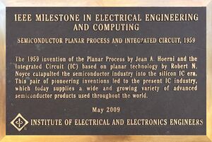
The 1959 invention of the Planar Process by Jean A. Hoerni and the Integrated Circuit (IC) based on planar technology by Robert N. Noyce catapulted the semiconductor industry into the silicon IC era. This pair of pioneering inventions led to the present IC industry, which today supplies a wide and growing variety of advanced semiconductor products used throughout the world.
Street address(es) and GPS coordinates
844 E. Charleston Rd., Palo Alto, CA 94303 (GPS: 37.421785, -122.103339); the original Fairchild Semiconductor HQ building from its founding in 1957.
Details of the physical location of the plaque
- The IEEE bronze plaque is installed on a marble stele resting on concrete in front of the building
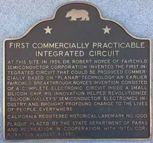
- Installed on its own marble stele to the left of the IEEE plaque is a second bronze plaque: California Historical Landmark #1000 titled "Site of Invention of the First Commercially Practicable Integrated Circuit" whose citation reads "At this site in 1959, Dr. Robert Noyce of Fairchild Semiconductor Corporation invented the first integrated circuit that could be produced commercially. Based on 'planar' technology, an earlier Fairchild breakthrough, Noyce's invention consisted of a complete electronic circuit inside a small silicon chip. His innovation helped revolutionize "Silicon Valley's" semicondutor electronics industry, and brought profound change to the lives of people everywhere."
How the intended plaque site is protected/secured
Building security; 24/7 access.
Historical Significance
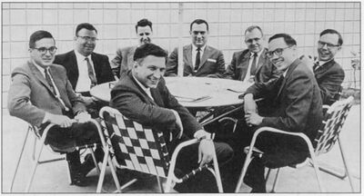
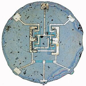
By the early 1950s, scientists and engineers first conceived of entire electronic circuits formed within a single block of semiconductor material. In the spring of 1959, several individuals filed key patent applications in pursuit of this goal. In his miniaturized electronic circuits, Jack Kilby of Texas Instruments used only one kind of material to fabricate all circuit elements. Kurt Lehovec of Sprague Electronics claimed the use of P-N junctions for the electrical isolation of such elements. At Fairchild Semiconductor, Jean Hoerni’s revolutionary planar process inspired Robert Noyce’s vision of interconnecting multiple elements on a chip without manual wiring. And late in 1959, Jay Last assembled a team whose creative efforts led in 1960 to the development of Fairchild Micrologic, the first planar integrated circuits and the forerunners of the modern world of microelectronics.
References
- US Patent 3,025,589 - Inventor: Jean A. Hoerni; filed on 1 May 1959
- US Patent 2,981,877 - Inventor: Robert N. Noyce; filed on 30 July 1959


