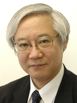
Hiroshi Iwai
- Associated organizations
- Tokyo Institute of Technology
- Fields of study
- Semiconductors
Biography
Hiroshi Iwai’s dedication to pushing the boundaries of integrated circuit scaling broke perceived barriers to enable the continued miniaturization of electronic devices providing higher performance with lower power that are integral to today’s mobile electronics. When industry forecasted that complimentary metal-oxide-semiconductor (CMOS) scaling wouldn’t go below 1 micrometer due to current leakage and lithography issues, Prof. Iwai provided solutions demonstrating that 25-nanometer (nm) scaling was possible. Among his many innovations, he developed technologies for shallow junctions and optical lithography to allow fabrication of 40-nm gate-length CMOS transistors. He also devised techniques for growing ultra-thin silicon oxide films to overcome leakage issues when using extremely small gate lengths. Overall, Prof. Iwai’s contributions demonstrated to industry that sub-50-nm CMOS scaling could be achieved.
An IEEE Life Fellow, Prof. Iwai is a professor with the Tokyo Institute of Technology, Yokohama, Kangawa, Japan.
