The University of Manchester MU5 Computer System
Contributed by Roland Ibbett, Emeritus Professor of Computer Science, University of Edinburgh, and previously Reader in the Department of Computer Science, University of Manchester. Figures 1, 5 and 6 are reproduced here by kind permission of that Department.
Introduction
MU5 was the fifth computer system to be designed and built at the University of Manchester under the leadership of Tom Kilburn.[1] When the Department of Computer Science was formed in 1964, the fourth Manchester computer, Atlas (inaurgurated in December 1962), was being used to provide a computing service for the University. Plans for the Department included significant expansion of research activity, beginning with the first year of Computer Science graduates in 1968. Experience had shown that research into hardware/system software could not be carried out on a computing service machine. It was excluded both by the nature of the work and by the excessive computing requirements of the simulation studies and the automation of hardware and software design which were dominant features of such research. So there was a need for an independent facility to support this research but, more importantly, a desire to continue the tradition of designing and building advanced systems, pioneering ideas which could be exploited by the computer industry.
An outline proposal for the new system was presented at the 1968 IFIP Conference in Edinburgh,[2] though talks with ICT aimed at obtaining their assistance and support began in 1966 (Ferranti, the company with which the University had collaborated to produce the Mark I, Mercury and Atlas computers, had by then become a part of ICT, which itself later became ICL). An application for a research grant was submitted to the UK Science Research Council (SRC) in mid-1967 and a sum of £630,446 spread over 5 years became available in January 1968.
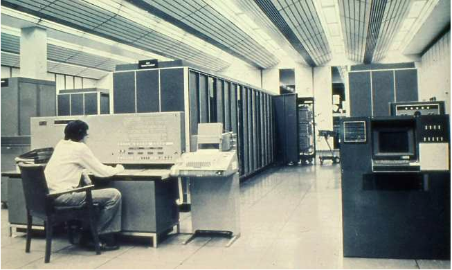
The feasibility of constructing a large computer system for this amount of money relied upon the availability of ICT's production facilities, at works cost price, at its nearby West Gorton factory. Even so, finance was a limiting factor, and it was accepted that the hardware produced would only be a small version (in architectural terms) of a potentially large system. Physically MU5 was a large machine, like most mainframes of its day, as can be seen from Figure 1.
Design Objectives
Many of the ideas embodied in MU5 grew out of experience gained from the Atlas project. The design objectives were set out in the grant application to the UK Science Research Council dated May 1967. Part of this application was for money to purchase a readily available commercial computer to initiate the project.
"The computer required is an ICT 1905E specially fitted with a 750 ns store... The 1905E will be transformed into a multi (initially 2) computer system by the addition of a completely new high-performance computer with a target throughput of 20 times that of Atlas ... It will be constructed by ICT (their agreement has been obtained) and will be charged at works cost price ... The 1905E, with the proposed modifications in view, will provide a vehicle which permits an immediate start on software developments aimed at the full system programs of the multi-computer system. The system programs will be written in a modular way to facilitate changes and extensions when these are required as the hardware develops."
The factor of 20 was to be achieved as follows:
- Integrated circuits and interconnection techniques would give a basic computing speed of seven times Atlas.
- A 250 ns cycle time store would be used (the Atlas core store had a 2μ cycle time).
- The design would include fast operand registers and register to register arithmetic (though these would not be addressable registers of the kind used in the CDC 6600, for example), and multiple arithmetic units (though, again, these would be different from those used in the 6600, being dedicated units rather than general purpose ones).
- An instruction set would be provided which would permit the generation of more efficient object code by the compilers. Particular attention was to be given to the techniques for computing the addresses of array elements and array bound checking would be provided as a hardware feature.
- The efficiency of the Atlas supervisor was approximately 60%. The provision of special hardware and the information obtained from a detailed study of the Atlas system over the previous two years would permit this efficiency to be significantly increased.
Items (1) to (3) were expected to give a factor of about ten, indeed the time for the inner loop of a scalar product was expected to be 1 μs as compared with 12 μs on Atlas. Items (4) and (5) were expected give at least a further factor or two.
What mattered was system throughput, rather than raw machine speed, and significant performance increases were to be sought from optimising the hardware to meet the software requirements. In this context it was anticipated that associative storage would play a significant rôle in the design; suitable integrated circuit elements were already being developed for this purpose.[3]
The processor to be built at the University was intended to be an example of a machine at the top end of a range of machines. The range was intended to go from machines of about PDP-11 cost to a multi-computer system incorporating several processors with differing biases (e.g. scientific or commercial) at the top of the range.
Software plans for the project were geared as much to the MU5 multi-computer system and the range concept as to the MU5 processor. To quote again from the grant application:
"The initial operating system will be for a single computer system but it will be extended to accommodate additional computers whose structures and order codes are different from those of the 1905E. It will be modular and easily changed in order to accommodate future hardware and software developments."
The detailed design of the operating system had not been completed at that time, but it was expected to have some form of file storage and on-line access, job queueing and scheduling for base load jobs, and priority routes through the system for urgent jobs. The basic kernel was to be kept to a minimum and most of the operating system facilities would run as non-privileged programs. Compilers were to be produced using ideas developed from the Atlas Compiler Compiler. The emphasis was to be on efficiency, compactness and machine independence.
Processor Design Considerations
Many of those involved in the project were new to the business of designing a real computer, and found themselves in an environment with much inherited wisdom, especially Tom Kilburn's, from previous Manchester projects. If there was a choice over some issue, "should it be like Atlas, or should it be different?", then there would have to be a good reason to make it different. The use of virtual addressing, for example, one of the most significant novel features of Atlas, was pretty much predetermined, though not before the virtues of real addressing (e.g. avoiding the address translation time delay and the ability to move complete logical entities such as procedures or arrays between levels in the storage hierarchy) had been re-considered.
There was never any real question of using a clock. Atlas had been asynchronous, for good reasons, so the new machine would be. In any case, it was going to be physically so big that it would not have been any use having a clock. Even in units of the system that ran semi-synchronously, using a series of asynchronously generated 'beats' that ran sequentially through several stages of the pipeline, parts of the logic ran sufficiently far behind the beat generation logic to create major problems in getting logical control signals back in time. Trying to stall the entire pipeline because of a data dependency, for example, would have been impossible. Furthermore, the time required to execute a floating-point addition was going to be data dependent, and limiting the speed of the machine to that of the slowest floating-point addition would have been unacceptable.
The prime consideration was the aim of ensuring fast, efficient processing of high-level language programs in an interactive environment. This requirement led to the need for an instruction set which satisfied the following conditions:
- Generation of efficient code by compilers must be easy.
- Programs must be compact.
- The instruction set must allow a pipeline organisation of the processor leading to a fast execution rate.
- Information on the nature of operands should be available to allow optimal buffering of operands.
Algol and FORTRAN were taken as being typical of two major classes of programming languages in common use at the time, distinguished by the use of recursive routines (or procedures) and dynamic storage allocation in the former, and non-recursive routines and compile time storage allocation in the latter, but having the following features in common:
- Each routine has local working space consisting of named variables of integer (fixed-point) and real (floating-point) types, and structured data sets (arrays, for example) which are also named.
- A routine may refer to non-local names either of an enclosing routine or in a workspace common to all routines.
- Statements involve an arbitrary number of operands which may be real names, array elements, function calls or constants.
In order to reconcile feature 3 with condition 1 and 4, it was decided that there would be an address form corresponding to each of the different operand forms. However, it was felt that to have more than one such operand specification per instructions would conflict with conditions (2) and (3). The option of using addressable fast registers to allow short instructions was also rejected. There were two arguments against registers. The first was the desire to simplify the software by eliminating the need for compilers to optimise their use. The second was the desire to avoid the need to dump and restore register values during procedure entry and exit and process changes. The alternative arrangement proposed for MU5 was a small, associatively addressed, selective cache memory that would hold values of named variables in current use, referred to as the Name Store.
The MU5 instruction set
To avoid tortuous grammatical constructs, the following description of the MU5 instruction set is written in the present tense, even though MU5 itself no longer exists.
The instruction format chosen for MU5 represents a merger of single address and stacking machine concepts. All the arithmetic and logical operations involve the use of an accumulator and an operand specified in the instruction, but there is a variant of the load order (*=) which causes the accumulator to be stacked before being re-loaded. In addition, there is an address form (STACK) which unstacks the last stacked quantity. Thus the expression
RESULT := (A + B) * ((C + D)/(E + F))
can be compiled into
ACC = A
ACC + B
ACC *= C
ACC + D
ACC *= E
ACC + F
ACC ∅ STACK
ACC * STACK
ACC => RESULT
The function ∅ is reverse divide (i.e. ACC = STACK/ACC); if the operand to the left of an operator is stacked, it subsequently appears as the right hand side of a machine function (as the dividend in this case). Thus, for the non-commutative operations - and /, the corresponding reverse operations have to be provided. In pure stacking machines, all subtractions and divisions are implicitly reverse operations.
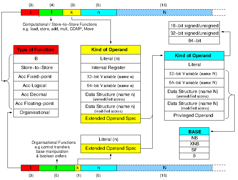
The instruction set is summarised in Figure 2. There are two basic formats, one for computational functions and one for organisational functions (control transfers, base register manipulations, etc.). They are distinguished by the type of function bits (t) and use four and six bits respectively to specify the function (f). The remaining nine or seven bits specify the primary operand. The k field indicates the kind of operand, and determines how the n field is interpreted. Where the k field indicates the Extended Operand Specification, the instruction is extended by a 16-bit N field in the case of a name, or by 16, 32, or 64 bits in the case of a literal.
The virtual address space is formally segmented: the unique identity of store words belonging to different processes is maintained by splitting the address into three separate fields, a 4-bit Process Number, a 14-bit Segment Number, and a 16-bit address defining a 32-bit word within a segment. Segments 8192 to 16383 are common to all processes, allowing a single copy of a compiler, for example, to be shared by all active processes. Scalar variables are normally held in a single segment of a process (normally segment 0) at addresses formed by adding the 6 or 16-bit name in the instruction to the contents of the Name Base register (NB). The name segment number and the process number (both held in special registers in the processor) are concatenated with these addresses to form the full virtual addresses required for store accessing. The value held in NB is unique to the name space associated with each procedure, and is altered at each procedure change. Accesses to names of other procedures and to common variables are made using the Extra Name Base (XNB), while using zero as base allows absolute addressing into the Name Segment (to access the Name Base values of different procedures, for example). The Stack Front register (SF) points to the area immediately beyond the name space of the current procedure, so that stacked variables are contained within the same address space as the names. SF is automatically incremented or decremented during the execution of a stacking function or a STACK operand access respectively.
Scalar variables can be of size 32 bits and 64 bits. They are accessed from the Name Store using an address formed by adding the name to the base register specified in the instruction (implicitly the Name Base in 16-bit instructions). The Name Store has two parts, 32 associatively accessed address registers and 32 64-bit value registers, so although a name + base address can point to a 32-bit variable, the base registers themselves can only point to 64-bit quantities. Thus the least significant bit of each of the base registers is set to zero and the name of a 64-bit variable is shifted left one place before being used to form an address.
Access to array elements is achieved through a descriptor mechanism. When a data structure element is specified by the k field, the corresponding primary operand is a 64-bit descriptor. This descriptor is sent to a D-unit within the processor, together with the contents of the B register if the k field specifies modification. The D-unit interprets the descriptor and makes a secondary store access for the element. This detachment of secondary addresses from instructions, and the use of names within instructions, allows the full 30-bit virtual address space available to a process to be referenced by 16-bit instructions.
There are two main types of descriptor:
String descriptor:  Ts  Length  Origin
Vector descriptor:  Tv  Bound   Origin
                     8    24     32
String descriptors describe strings of bytes. The length field specifies the number of bytes, and the origin specifies the byte address of the first byte. Strings are normally used in conjunction with string processing orders (which may be two-address operations involving the use of two descriptors). These orders provide facilities for the manipulations of data records in languages such as COBOL, PL/1 and Algol 68 (move, compare, logically combine, etc.).[4]
The size of the elements in a vector is specified within the type bits (Tv) and may be between 1 and 64 bits. If the operand access is modified, the modifier must be greater than or equal to zero and less than the bound. This check is carried out automatically by hardware with virtually no time penalty, and removes the need for the costly software bound check which is often required, particularly during program development.
Hardware Design
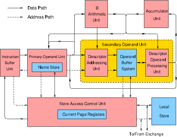
The design of the hardware of the MU5 processor initially centred around the Name Store and the descriptor mechanism. The special associative circuits designed for the Name Store were expected to be capable of operation in 70 ns, but an additional 70 ns was necessary to read the value from the RAM used to hold the actual operand values (later to become nominally 40 ns in both cases). However, it was believed that a fixed-point arithmetic unit could be constructed to perform simple functions such as addition and subtraction in just under 50 ns, using the technology from which MU5 was to be built, and so clearly the two activities in the Name Store would have to be overlapped if the store speed was to approach the arithmetic speed. Furthermore, the addition of the name to the base register contents would also require a comparable amount of time, and so the hardware required to access a primary operand developed into a 5-stage instruction pipeline,[5] known as the Primary Operand Unit (PROP). PROP would receive instructions at its input and supply at its output functions and primary operands ready for execution or further interpretation by the descriptor system.
To access secondary operands using the descriptor mechanism required two logically distinct pieces of hardware, one to form addresses (the Descriptor Addressing Unit) and one to select the operand from within the corresponding store word (the Descriptor Operand Processing Unit). Together with an Operand Buffer System[6] which sat between them, these units formed the Secondary Operand Unit (SEOP).[7]
The Accumulator unit (containing principally the floating-point execution hardware) clearly had to be placed after SEOP in the overall design of the Processor, since it would be processing the array elements accessed by the SEOP. The B-unit, on the other hand, was better placed close to PROP, in parallel with the Descriptor Addressing Unit, since it was to supply modifier values, and would, therefore, operate mostly on named quantities rather than array elements.
Thus the final configuration of the Processor became that shown in Figure 3. The Primary Operand Unit was supplied with instructions by the Instruction Buffer Unit (IBU), and the virtual to real address translation took place within the Store Access Control Unit (SAC), which coordinated requests to the Local Store. SAC also developed into a pipeline structure, to keep pace with the demands of the other units.
Instruction Accessing
The IBU was designed to be able to supply instructions to PROP at the required rate using a pre-fetching mechanism. Although MU5 was asynchronous, there was a minimum 'beat' time in the PROP pipeline and this was expected to be 40 ns, so the maximum required instruction rate was 400 Mbps. The main store, a 250 ns cycle-time plated-wire system, was to be constructed of 128-bit wide stacks, and would therefore be able to supply, without interleaving, 500 Mbps. Interleaving would improve this rate, so that even allowing for operand accesses (and the Name Store would intercept most of these), there would be no problem in supplying instructions at the required rate.
The real problem was branches (control transfers in Manchester terminology). These were expected to occur on average once every ten instructions, and would create long gaps in the instruction stream because, despite the high data rate, the store access time was comparatively long. The MU5 team was aware of techniques developed by IBM and CDC to deal with this problem, particularly those which involved loop catching, but wanted to avoid solutions which were constrained by hardware limitations on loop size.
Various alternative solutions were considered, and simulation studies undertaken. The solution chosen was based on a Jump Trace mechanism[8] (effectively a jump history table), which attempted to predict the result of an impending control transfer instruction and thus prefetch the instructions required for a loop, rather than catch the loop in a high-speed, size-limited buffer. The simulation studies showed that it was possible to provide the correct sequence of instructions following control transfers in about 65% of cases using an 8-line Jump Trace. The Jump Trace was updated whenever a previously unencountered branch occurred, and as each pre-fetch address was generated, it was compared with the contents of the Jump Trace. If a match was found, the previously 'jumped-from' address was substituted with the 'jumped-to' address and prefetching continued from this new address. An extra digit carried through the pipeline with each pre-fetched instruction told the branching logic whether or not the instruction following a branch was 'out-of-sequence', i.e. whether it had been predicted or not.
Arithmetic performance
The instruction set allowed for the possibility of fixed-point, floating-point and decimal arithmetic in the main Accumulator Unit, but no decimal hardware was actually included in MU5. At the outset of the design it had been assumed that it would be possible to build a floating-point unit in which addition (or subtraction) would take not more than about twice as long as a fixed-point addition in the B-unit.[9] In practice this turned out not to be the case. A fixed-point addition took about 50 ns, as predicted, whereas the (data dependent) time for floating-point addition was about 250 ns on average.
This disappointing performance could not have been improved by pipelining. Although instruction processing was heavily pipelined in MU5, there would have been no point in pipelining the arithmetic unit, since in any one-address computer, the result of one arithmetic operation is required as an input to the next, and so all but one of the pipeline stages would always be empty.
The MU5 Complex
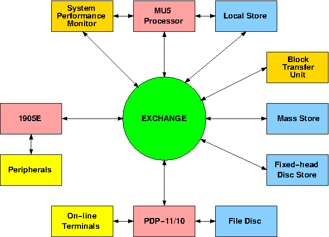
The MU5 Processor and its Local Store actually formed two units of a larger system, the MU5 Complex (Figure 4), an integrated system in which the operating system and other software was distributed among several computers. Communication between different parts of the software, which involved the transfer of both pages of data and short messages between the computers in the complex, was implemented in software via a formalized message switching system.[10] These transfers were implemented in hardware by an 'Exchange',[11] which allowed single 64-bit parallel word transfers between up to a dozen units at a rate of one every 100 ns.
Both the MU5 Processor itself and its Local Store were connected to the Exchange. The Mass Store acted both as a buffer area for data transfers between processors and as the first level of backing store for the Local Store. It consisted of two stacks of 2.5 μs core store, each containing 128K words of 32 bits. Transfers of blocks of data between the Mass and Local Stores were made under the control of an autonomous Block Transfer Unit (BTU). Once initiated, the BTU generated the necessary requests, via the Exchange, to the Mass and Local Stores to carry out the transfer. The next level of backing store was the (8 Mbyte) Fixed-head Disc,[12] which had its own block transfer unit.
The ICL 1905E computer served a number of purposes during the MU5 project. Initially it was used to simulate both the hardware and software of the MU5 Processor. Simulation of the hardware, without which the project could never have been undertaken, was carried out at logic gate level, for separate groups of MU5 logic, using a suite of purpose-designed programs.[13] Simulation of MU5 software was facilitated by the provision of a paging system, which itself acted as a test bed for the associative circuits to be used in the MU5 processor.
Once the system became operational, the 1905E became the main peripheral handling processor in the complex and was fitted with standard devices such as lineprinters, tape readers, etc. Additional peripheral handling capability was provided by the PDP-11/10 processor, which was originally installed to act as a file disc controller, but which later also supported the on-line terminals.
The System Performance Monitor (SPM) was a special purpose monitor developed in MU5 technology. As well as sixteen 32-bit counters, the SPM incorporated a 512 word 16-bit store, and various modes of operation enabled different types of histograms to be recorded in this store. Because the SPM was connected to the Exchange, it could be controlled by software in MU5 and as one of the digits in the MU5 machine status register gated the SPM's inputs, processor activity in a single process or even parts of a process could be monitored.
Technology
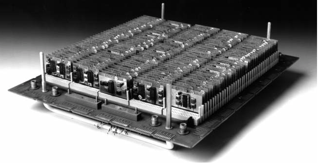
It was clear from the outset of the project that the Department would not be able to build the system in-house, so that it would be essential to use commercial production facilities and hence commercially available technology. The fastest form of logic technology available at the time was Emitter Coupled Logic (ECL), a particular version of which (MECL 2.5) was being using by ICT to build a processor at the top end of its 1900 range, the 1906A. MECL 2.5 technology involved the use of small-scale integrated logic circuits (manufactured by Motorola) mounted on small printed circuit boards known as modules. Modules were interconnected by insertion into sockets mounted on multi-layer 13in x 16in 'platters' each with a capacity of up to 200 modules (Figure 5). Although the interconnection layers were buried inside the platters, connections to the module sockets were brought up to the surface so that they could be cut, if there were design or manufacturing errors, and replaced with wires. Provided these were close to the surface, their transmission line characteristics were within acceptable limits. The module connection pins also allowed oscilloscope probes to be attached to virtually any logic signal within the system.
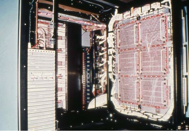
The platters were housed in bays, each capable of holding 33 platters, one fixed group of nine in the centre of the bay and four groups of six mounted on double-sided swing out 'logic doors' (Figure 6). Two such bays made up the MU5 Processor. Other bays held the Local Store, the Exchange, the Fixed-head Disc Store (the Mass Store came in its own free-standing cabinet) and power supplies. The complete system involved about 100 platters.
Interconnections between platters within a group were made by means of pressure connectors along adjacent edges, whilst connections between groups of platters and between bays were made through co-axial cables. The co-axial cables were terminated on small printed circuit boards which were themselves connected to the platters by pressure connector along the outer edges of each group.
The total power consumption was of the order of 30 KW. To remove the heat generated by this amount of power, the module sides of the platters were enclosed in 'chimneys' and chilled air was blown down the chimneys. The chilled air was provided by heat exchangers at the ends of the bays, themselves supplied with cold water. The heat carried away by this water was used to heat the building in cold weather or dispersed into the atmosphere through heat exchangers on the roof in warm weather.
Commissioning and Beyond
Commissioning (i.e. making the hardware and software do what they were supposed to do) started in earnest in the summer of 1971 when the first platters were delivered from West Gorton. By then all the mechanical work involved in installing the cabinets, power supplies and inter-bay wiring had been completed, in the room in which the original Mark I computer had been built. However, in 1972, the system was dismantled and transferred to the new Computer Building (now the Kilburn Building) which had been built to house the Computer Science Department and the University of Manchester Regional Computing Centre (UMRCC). The MU5 team were the first occupants of the building.
Once it became fully operational, MU5 ran a valuable computing service for up to 25 active on-line users (out of a user community of about 100) in the Department until it was dismantled in 1982.
MU5 was a major influence on the ICL 2900 series, although at the time of its announcement, ICL made no reference to the MU5 contribution, even though John Buckle, a member of the original ICL architectural design team for the 2900 Series, writing in his book on the ICL 2900 Series,[14] said:
"the single most important external influence on the 2900 architecture was almost certainly the Manchester University MU5 system." It was not until the Golden Anniversary Conference held in Manchester in June 1998 to celebrate the 50th anniversary of Mark I running the world's first digital electronic stored program, that ICL publicly acknowledged the contribution of the MU5 project to the design of the 2900 Series, thus recognising the importance to the British computer industry of what was probably the largest computer project ever undertaken in a British University.
See also
- Experiences with the Membrain 7700, a first-hand account by Tanj Bennett working with the Membrain 7700, a computer that was effectively a minicomputer version of the MU5
Bibliography
This bibliography lists some of the many papers written about MU5. Most of the material presented here has appeared in [15], [16] and [17].
- ↑ https://en.wikipedia.org/wiki/Tom_Kilburn
- ↑ T. Kilburn, D. Morris, J.S. Rohl & F.H. Sumner, "A System Design Proposal". Information Processing 1968, Vol 2, pp 806-811, North Holland, 1969.
- ↑ D. Aspinall, D.J. Kinniment & D.B.G. Edwards, "Associative Memories in Large Computer Systems". Information Processing 68, Vol 2, pp 796-800, North Holland, Amsterdam, 1969.
- ↑ P.C. Capon, R.N. Ibbett & C.R.C.B. Parker, "The Implementation of Record Processing in MU5", IEE Conference Proceedings, No. 121, 1973.
- ↑ R.N. Ibbett, "The MU5 Instruction Pipeline". Computer Journal, Vol 15, pp 43-50, 1972.
- ↑ J.V. Woods & F.H. Sumner, "Operand Accessing in a Pipelined Computer System". IEE Conference Proceedings, Vol.121, pp 326-43, 1974.
- ↑ J. Standeven, S. Lanyado, & D. B.G. Edwards, "The MU5 Secondary Operand Unit". IERE Conference Proceedings, Vol. 25, pp 429-440, 1972.
- ↑ F.H. Sumner, "MU5 - An Assessment of the Design". Information Processing 74 North-Holland, Amsterdam, pp 133-136, 1974.
- ↑ J.B. Gosling, "Review of High-speed Addition Techniques". IEE Proceedings, Vol 118, pp 29-35, 1971.
- ↑ D. Morris, G.R. Frank & T.J. Sweeney, "Communications in a Multi-computer System", IERE Conference Proceedings, Vol. 25, 1972, pp 405-413.
- ↑ S.H. Lavington, G.Thomas & D.B.G. Edwards, "The MU5 Multicomputer Communication System", IEEE Trans. Computers, C-26, 1977, pp 19-28.
- ↑ D.B.G. Edwards, A.E. Whitehouse, L.E.M. Warburton & I. Watson, "The MU5 Disc System", IEE Conference Proceedings, No 121, 1974.
- ↑ H.J. Kahn & J.W.R. May, "The Use of Logic Simulation in the Design of a Large Computer System", IERE Conference Proceedings. Vol. 25, pp. 19-30, 1972.
- ↑ John K. Buckle, "The ICL 2900 Series". The Macmillan Press, London, 1978.
- ↑ R.N. Ibbett & P.C. Capon, "The Development of the MU5 Computer System". Communications of the ACM, pp 13-24, 1978.
- ↑ Derrick Morris & Roland N. Ibbett, "The MU5 Computer System". The Macmillan Press, London, 1979.
- ↑ R.N. Ibbett, "The University of Manchester MU5 Project". IEEE Annals of the History of Computing, Vol. 21, No1, pp 24-33, 1999.
