Microwave Circuits
Microwave systems, such as radars, and radio and other communication devices are made of many electronic parts called “circuits” or “components.” These are designed and constructed to manipulate electromagnetic phenomena into carrying out different microwave signal processing functions such as generating, modulating, controlling, and amplifying signals. They are also used in frequency translation (conversion). The construction of such electronic circuits is usually quite different from those used in low-frequency equipments, such as television sets or AM/FM radio, for example.
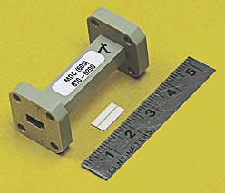
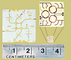
In the early development of microwave circuits and systems (during and just after World War II) heavy and bulky microwave circuits in the form of voluminous, hollow metallic pipes and tubes (called waveguides) were used. These large, three-dimensional waveguides are still in use today for certain high-power applications. However, since the 1960s, planar transmission line circuits (or planar circuits, which are referred to as two-dimensional flat-surface layered topologies) have been the more popular choice. They are relatively cheap, lightweight, and can be made very small (the principle of miniaturization). Also in the 1960s, the concept of microwave integrated circuits (MICs) was introduced. Instead of building individual microwave components separately and then connecting them on a piece-by-piece basis, it was thought it would be more cost effective and mass-producible to laminate or “print” an entire circuit on a single planar dielectric substrate (that looks like a small, flat chocolate chip) with various components connected to each other (usually by soldering) in a continuous integrated fashion.
A planar circuit always consists of a number of specific, but carefully dimensioned, very thin, metallic line and/or slot patterns that are formed on or between planar dielectric substrates. These metal lines or patterns connect microwave components such as transistors, resistors, and capacitors, and may perform other circuit functions. Typically, the thickness of those conducting patterns is around 0.5 micrometer through 50 micrometers (about the thickness of fine paper, such as tissue paper). The substrate thickness ranges from 50 to 1000 micrometers (about the thickness of a compact disk), depending on the processing technique and user requirements.
If a MIC is fabricated on a non-semiconductor substrate such as alumina (ceramic) and low-loss plastics, microwave diodes and transistors as well as other “active” and “passive” components may be mounted on the substrate to realize a specific application. Such a resulting circuit is usually referred to as a hybrid MIC. Integrated parts on the substrate only deal with passive functions (passive components) such as filter and power divider, which process the microwave signal in their own ways without additional (external) electric intervening. Of course, all the parts, including the active ones, can be completely integrated on a single “chip” with semiconductor technology. The circuit thus becomes a monolithic MIC (MMIC). The MMICs are today’s preferred choice for size miniaturization and mass production, as they can be made much smaller than the hybrid MIC. A typical MMIC chip is about the size of the shirt’s small button (although they’re usually rectangular), and require the use of a microscope to see fine details of its electronic pattern.
Generally, the size of a microwave planar circuit is directly proportional to a certain “average” value of wavelengths “seen” by the transmission lines (effective wavelength). This is inversely proportional to the operating frequency. Its size also depends on the dielectric constant of the substrate. Further miniaturization of the circuit can be made by many techniques such as the use of a high dielectric constant substrate. In this way, the “effective wavelength” becomes shorter, and the circuit can be made smaller.
Now there are many new techniques used for making more and more small, compact, and complex circuits. One well-known example is to design three-dimensional high-density MICs in which many layers of circuits are vertically stacked. It is hoped that in the future it will be possible to fabricate a complete and very cheap microwave system on a single planar-layered chip.

