Leo Esaki
- Birthdate
- 1925/03/12
- Birthplace
- Osaka, Japan
- Associated organizations
- Sony Corporation, IBM
- Fields of study
- Semiconductors
- Awards
- IEEE Medal of Honor, Nobel Prize in Physics, Nishina Memorial Award, Morris N. Liebmann Memorial Prize, Stuart Ballantine Medal, Japan Academy Award, Order of Culture from the Japanese Government
Biography
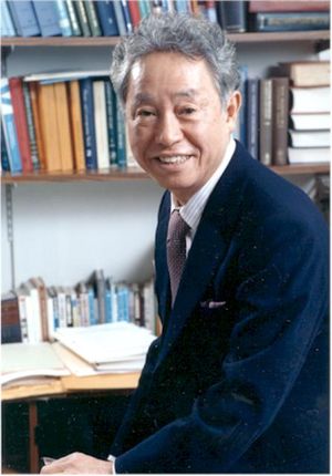
Leo Esaki was born on 12 March 1925 in Osaka, Japan. He is one of only three Japanese physicists ever to receive the Nobel Prize. Interestingly enough, all three attended the Third High School (equivalent to the present junior college) in Kyoto, which may be no more than just coincidence or proof of the importance of an educational environment in developing scientific talent.
Esaki went on to major in physics at the University of Tokyo because he wanted to understand nature in a most fundamental way, but credits the war-time psychology as also having an effect on him, especially after the war. It was then that he decided to go into industrial research, in order to participate more effectively in the process of rebuilding war-torn Japan. He joined Sony Corporation, and it was there in 1957 that he discovered the tunnel diode, the first quantum electron device, for which he received a Ph.D. in physics and, later, the 1973 Nobel Prize in physics.
Other awards related to this discovery include the Nishina Memorial Award (1959), the Morris N. Liebmann Memorial Prize from IRE (1961), the Stuart Ballantine Medal from the Franklin Institute (1961), the Japan Academy Award (1965), and the Order of Culture from the Japanese Government (1974).
In 1960, motivated by his curiosity about American ingenuity and perhaps the American dream, he came to the U.S. and joined IBM Research. An offer from IBM to become a resident consultant extended what was to be a one-year visit into a stay that has lasted 31 years. In 1967 he was named an IBM Fellow.
For more than twenty years, Esaki's work at the IBM /T. J. Watson Research Center has focused on man-made semiconductor structures such as superlattices and quantum wells. The origins of such structures date back to seminal papers by Esaki and Raphael Bu, published in 1969 and 1970. They asserted that semiconductor structures of extraordinary electronic properties could be designed using the principles of quantum theory and synthesized with the advanced techniques of epitaxy - "do-it-yourself quantum mechanics, " or "band structure engineering." In the last decade, this interdisciplinary field has witnessed phenomenal growth. A variety of engineered structures have demonstrated intriguing characteristics, including nearly ideal resonant tunneling. Activities in this new frontier of semiconductor science have given immeasurable stimulus to device design, leading to unprecedented electron-transport and optoelectronic devices for applications.
In recognition of his pioneering role in opening up this new field, known as semiconductor quantum structures, Esaki shared with his two colleagues the 1985 International Prize for New Materials of the American Physical Society. In 1991, he was awarded the IEEE Medal of Honor, "For contributions to and leadership in tunneling, semiconductor superlattices, and quantum wells."
Esaki is a Fellow of the American Academy of Arts and Sciences, and a Foreign Associate of both the National Academy of Sciences and the National Academy of Engineering. In addition to his scientific achievements, Esaki has also helped interpret Japan for the West and vice-versa. Through his witty essays, he has helped bridge the gap between the two cultures that he, as a scientist with a foot in each, has managed to span. Esaki retains close ties with his homeland, visiting several times a year. He is a Director of IBM-Japan, a Member of the Japan Academy, a Director of the Yamada Science Foundation, and an adjunct professor of the Waseda University.
