Scanning Probe Microscopy
This article was initially written as part of the IEEE STARS program.
Citation
Probe microscopes are a class of techniques that can image surface features at the nanometer or even atomic scale. They were invented in the early 1980s for basic research and quality control for microelectronics manufacturing, and they are still used in semiconductor and magnetic memory R&D and manufacturing. However, the community that formed around them has shown enormous creativity in adapting them for use in other industries and in a variety of academic disciplines. Their utility across disciplines and industries makes them one of the most important classes of instrumentation in the emergence of the global nanotechnology enterprise.
Introduction
For almost a half-century, commercial semiconductor manufacturing has followed a steady trend of miniaturization known today as Moore’s Law. This “law” – really, more of a rough rule of thumb and mechanism of industrial coordination – observes that the number of integrated circuit components that can profitably be crammed on a commercial wafer doubles approximately every two years. As a result, some features on commercial chips are now only a few atoms wide. On almost all state-of-the-art commercial chips one can find features that are only a few nanometers – billionths of a meter – in size.
Moore’s Law proceeds because electrical engineers and practitioners of many other disciplines have been ingenious in inventing new ways to fabricate ever smaller features out of silicon and other materials. Fabrication technologies, however, are not the whole story. To successfully and consistently make smaller features, practitioners also need to see and characterize what they have made. Thus, Moore’s Law also depends on innovation in microscopy and other kinds of instrumentation.
Optical and electron microscopy – techniques that predate modern microelectronics – have been improved significantly in the past half-century in order to aid the semiconductor industry. However, the needs of microelectronics manufacturers have also stimulated the invention of entirely new classes of microscopes. None, perhaps, has been more important than the scanning probe microscopes, a class which now includes several variants regularly used in the microelectronics industry: scanning tunneling microscopes (STMs), atomic force microscopes (AFMs), magnetic force microscopes (MFMs), scanning capacitance microscopes, and other more exotic tools. Yet even though microelectronics manufacturing provided the incentives, resources, and personnel that led to the invention of many scanning probe microscopes, these tools are today used across a wide array of industries and academic disciplines. Probe microscopy’s evolution is a wonderful example of innovation through cooperation among researchers in industry, government, and academia, and through mutually beneficial relationships among applied and basic research fields.
First Steps
Probe microscopes, in general, work by bringing a small, solid tip, the “probe,” very close to a surface and then rastering or “scanning” the probe over the surface while measuring some interaction between probe and surface. The type of measured interaction defines the microscope variant: STMs measure the current of electrons that quantum mechanically “tunnel” between probe and sample; AFMs measure the van der Waals and other attractive and repulsive forces between the sample and a tip that is mounted on a flexible cantilever; MFMs measure the forces between magnetic domains in the sample and a magnetized AFM tip; etc. The strength of the tip-sample interaction is then converted into a z-value associated with the x-y coordinates of the tip over the sample. The combination of x, y, and z values is then converted into a three-dimensional picture of the surface, typically via software.
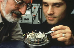
Today’s probe microscopy research community usually traces the origin of the technique back to 1981, when Heinrich Rohrer and Gerd Binnig, researchers at the IBM laboratory near Zurich, invented a rudimentary version of the scanning tunneling microscope with help from technical staff, most notably Christoph Gerber. (See Fig. 1) There were, however, precursor technologies that contained all of the prerequisites of a scanning probe microscope. A friend of the inventor of one of those precursors put it in the title of a rather peeved letter to Physics Today, “STM Not Invented in a Vacuum.”
Despite those precursors, Binnig and Rohrer deserve credit for a string of achievements. They were not the first to observe metal-vacuum-metal electron tunneling, but they appear to have been the first to do so reliably, and to document their results publicly enough to draw attention to their technique. They were also the first to image a surface by rastering a probe while measuring a tunneling current rather than a current of field-emitted electrons. Because a tunneling current is measurable only when the tip and sample are separated by a very small distance, scanning while tunneling is extraordinarily difficult to achieve, since scanning makes it more likely that stray vibrations will cause the tip to crash into the sample. Finally, while the STM was not the first microscope with atomic resolution (resolving power sufficient to distinguish the positions of atoms in a sample), it does appear to have been the first instrument to resolve single atoms (as opposed to columns of atoms) on flat surfaces of general scientific interest.
Binnig and Rohrer’s qualifications as inventors of a new technique stem in part from these technical breakthroughs. Just as important, though, was the fact that they took the microscope they had created and cultivated a community of researchers who would build their own STMs, consume STM data, articulate theories of how STMs worked, invent STM variants, develop new STM applications, share knowledge of how to build and use STMs, and eventually established institutions for bringing STMers together. Identifying precursors of the STM is not particularly useful for assigning credit for “firsts.” Instead, we should look to the STM’s predecessors to understand why an STM community did not form earlier and how the STM community succeeded when it did form.
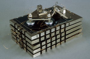
The most obvious of these predecessors was the “Topografiner,” invented by Russell Young at the U.S. National Bureau of Standards in the late 1960s. (See Fig. 2) The Topografiner contained the essential elements of an STM, but Young was able to operate it only in field emission mode, where the tip and sample are further separated than in an STM and the electrons travel ballistically between tip and sample rather than tunneling from one to the other. Young’s protégé, Clayton Teague, did succeed in the mid-1970s in operating the Topografiner in tunneling mode, but only while holding the tip stationary.
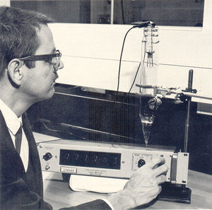
Young and Teague never arrived at a fully functional STM in part because the Bureau of Standards was, at the time, under intense pressure from Congress to cut back on basic research and to focus on short-term service to industrial customers. Senior Bureau administrators saw the Topografiner as a “high science” experiment, and were therefore unwilling to direct scarce resources to it. Outside the Bureau, however, researchers who might have tried to build their own Topografiners were unaware of Young’s difficulties with his supervisors. Instead, those few who had heard of the Topografiner simply assumed that if a researcher as competent as Young had not succeeded at building a tunneling microscope, then no one could. Indeed, Binnig and Rohrer were lucky not to know about the Topografiner until after they had already built a working STM, otherwise they might have been deterred in the same way others were.
The expansion of the STM community and the development of STM technology also benefited from the expertise of specialists in techniques more distantly related to the STM than the Topografiner – techniques whose practitioners Young had been unable to interest in the Topografiner. For instance, several very early STMers, notably Paul Hansma and Bob Jaklevic, came out of electron tunneling spectroscopy. Stanford’s Calvin Quate, who later co-invented the AFM along with Binnig and Christoph Gerber, brought his expertise in scanning acoustic microscopy – a technique still used for process quality control by some semiconductor foundries. Bell Labs’ Jene Golovchenko, perhaps the first person outside IBM to build a working STM, was attracted to the technique because of his prior experience with X-ray diffraction experiments that used piezoelectric positioners – the same means used for moving the STM probe around. A few early STMers were also practitioners of field ion microscopy, the first technique that could image individual atoms, though only in very sharp geometries, and just for tungsten and a few other materials. In fact, Russ Young’s Ph.D. advisor, Erwin Müller, had invented the field ion microscope.
Curiously, electron microscopists were not particularly important in the development of probe microscopy. Many people at IBM, including Binnig and Rohrer, thought that electron microscopists were the natural group to replicate the STM, but the few electron microscopists who tried to build early STMs were unsuccessful. More fundamentally, the STM’s small field of view, and (in general) ability to image only the outermost atoms of a surface, meant that the data it could generate were not immediately of interest to scanning electron microscopists, who image a much larger field of view, nor to transmission electron microscopists, who image through a sample rather than just at its surface. Over time, STM and electron microscopy became complementary techniques. However, the early expectation at IBM was that this complementarity would be achieved more quickly, and with a greater merging of the communities dedicated to these techniques.
A Community Forms
As it turned out, the most important constituency for the first STMs was the surface science community. This was somewhat unexpected, as neither Binnig nor Rohrer were themselves surface scientists. They originally conceived the STM both as an experiment for basic electron tunneling spectroscopy research and as a potential tool for characterizing thin films in the manufacture of a superconducting supercomputer that IBM was heavily committed to in the late 1970s. However, once they had built the first STM, Binnig and Rohrer began asking colleagues what samples they should characterize with it. Since IBM Research was at the time one of the leaders in semiconductor surface science, Binnig and Rohrer were soon directed to samples of interest to that field.
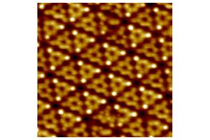
In particular, surface scientists suggested they use the STM to image the silicon (111) 7x7 “surface reconstruction.” Silicon (111) is a crystallographic notation for a piece of silicon in which bulk silicon’s natural diamond cubic unit cell has been cleaved along a plane that bisects each of the three orthogonal faces that touch any corner of the cell. Under different conditions and treatments, the surface layers of a silicon (111) crystal will reconstruct in a variety of ways, each of which is represented as a vector multiple of the “surface unit cell,” or a two-dimensional rendering of the underlying three-dimensional bulk unit cell. Typical reconstructions for silicon include 2x1 or √3x√3. The 7x7 is a reconstruction that is seven times longer than a silicon (111)’s surface unit cell along each of its characteristic vectors – an especially large and complex reconstruction.
Surface scientists knew that the 7x7 was an unusual reconstruction from indirect techniques such as low-energy electron diffraction, but after decades of research and dozens of attempts they were unable to pin down just where the atoms were. After trying other surface reconstructions and getting very little attention for their results, the STM team decided to place their bet on the 7x7. By early 1983, the gamble had paid off – they generated atomic resolution images of the 7x7 that instantly sent shockwaves through the surface science field and then through the general scientific community.(See Fig. 3)
Before the 7x7, only a few brave, mostly junior, scientists had attempted to replicate the STM, with little success. After the 7x7, senior surface scientists, especially at Bell Labs and IBM, threw money and personnel into catching up with the Zurich team. It was the first atomic resolution STM images of the silicon 7x7 that led to Binnig and Rohrer’s sharing the 1986 Nobel Prize in Physics with Ernst Ruska, one of the inventors of electron microscopy. That year also saw the first meeting of the International Conference on Scanning Tunneling Microscopy, where first dozens and eventually hundreds of probe microscopists began gathering every year at sites around North America, Europe, and Asia.
Variation and Improvement
The first atomic-resolution images of the 7x7 kicked off the rapid expansion of the probe microscopy community. (See Figs. 4 and 5)
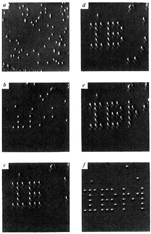
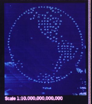
Other factors, however, were critical to sustaining that explosive growth. Significant innovation was required to turn probe microscopy into a technique that many disciplines and industries wanted to – and could – use. (See Fig. 6)
Binnig, Rohrer, Gerber, and early converts such as Paul Hansma at the University of California, Santa Barbara, and Calvin Quate at Stanford developed modifications to the original STM that made its operation considerably more reliable and user friendly. For example, by shrinking the size of the microscope they made it less prone to vibration. They also developed variants that could image a wider range of samples and would thereby appeal to a wider user base.
Foremost among these variants was the atomic force microscope. In 1985-86, Binnig took a sabbatical at Stanford to work with Calvin Quate’s group in Applied Physics and Electrical Engineering, while Gerber was temporarily assigned to the IBM laboratory near San Jose. Together, they brainstormed ways to overcome what they perceived as two of the STM’s biggest flaws – that it could not image insulating materials, and that it was of dubious use when operated in air rather than vacuum. These were not major problems for surface scientists, who were mostly interested in metals and semiconductors in vacuum. Binnig, however, was already looking for ways to use the STM in chemistry and biology. Meanwhile, Quate’s deep connections to Silicon Valley prompted him to look for ways the STM could be used in inspecting integrated circuits, where many important features are made from silicon dioxide and other insulators, rather than metals or semiconductors.
Their solution was to scan a small, flexible cantilever with a weight at the end (often, initially, a small diamond) over the sample while a stationary STM tip measured the deflection of the cantilever as it passed over features on the sample surface. At first, this “atomic force” microscope was not promising, but over the next two years two developments established it as a revolutionary means of inspecting nanoscale features. First, Quate’s group borrowed techniques from Silicon Valley to microfabricate standardized cantilevers. Second, Paul Hansma’s group (and, independently, Gerhard Meyer and Nabil Amer at IBM) used a laser-based optical lever scheme to replace the STM as a means of detecting cantilever deflection. Both innovations made the AFM easier to use and its images easier to interpret.
Demographic and Policy Shifts
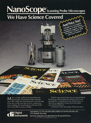
The late 1980s also saw the founding of commercial probe microscope manufacturers, especially in the US West and Southwest. In particular, Digital Instruments of Santa Barbara sold almost three hundred copies of a simple air STM between 1987 and 1990, essentially doubling the size of the probe microscopy community on its own. (See Fig. 7)
Almost all the successful STM and AFM companies of this period had some tight technology transfer relationship back and forth with one or two academic groups, and several of these companies were founded by professors. Established firms such as IBM and Bell Labs, in microelectronics, or Zeiss and JEOL, in microscopy, either did not attempt to sell probe microscopes or tried with little success.
Probe microscopy is therefore a prime example and, in small ways, a driver of the large-scale changes overtaking American and global R&D at the end of the Cold War. Academic physicists and electrical engineers, like their more famous colleagues in molecular biology, were increasingly founding start-ups and patenting their work in this period. High-tech companies, meanwhile, were moving away from vertical integration and deep commitments to in-house basic research. IBM and Bell Labs were the leading organizations in the first years of probe microscopy, but in the early 1990s they slimmed their research arms considerably. As a result, many corporate probe microscopists left for university appointments. Those who remained often felt pressure to focus on more near-term, applied topics. It was in that environment that new variants, such as the scanning capacitance microscope, the lateral force microscope, and the non-contact AFM, were invented that could help microelectronics companies improve the manufacture of integrated circuits and magnetic storage media.
The combined result of academic commercialization, decline of corporate in-house basic research, and improvements in the capabilities and operability of probe microscope technology was that the demographics of the probe microscopy community shifted quickly in the early 1990s. Many more users bought than built their microscopes; more came from universities than firms; and somewhat more were using their microscopes for applications in chemistry, the life sciences, and geology. Often, practitioners from the life sciences and other disciplines were drawn into probe microscopy by physicists and electrical engineers such as Binnig, Quate, and Hansma, who would invite representatives of those disciplines to collaborate and spend time in their labs. These interdisciplinary forays by engineers and physicists were not always successful, but they usually piqued enough interest that their collaborators’ disciplinary colleagues would begin buying STMs and AFMs. Thus, probe microscopy exemplified yet another trend in post-Cold War science: the increasing prevalence of interdisciplinary collaboration.
Instrumental Community
The interdisciplinarity and commercial outlook of academic probe microscopy in turn put the field at the center of emerging nanotechnology initiatives in the US and other industrialized nations in the late 1990s and early 2000s. The term “nanotechnology” was popularized in the late 1980s by Eric Drexler, a “speculative engineer” with close ties to Silicon Valley and the futurist and space enthusiast movements. By the early 1990s, journalists and science fiction writers had repeated the word often enough that elite scientists and members of the Clinton administration latched onto it as a label for a new science policy initiative. The point of this initiative was to offer federal support for the various shifts outlined above: greater university-industry collaboration, more interdisciplinary research, more sharing of expensive research tools, etc. The main tool of this initiative was to be a portfolio (more than sixty in 2013) of federal and university interdisciplinary centers that would hopefully fill the niche once occupied by Bell Labs and other giant corporate research centers.
In many countries, probe microscopy served as a much-heralded model for what “nanoscience” should look like. Probe microscopes, after all, can image and even manipulate nanoscale, or smaller, features. More subtly, the probe microscopy community was already doing many of the things that government nanotechnology initiatives encouraged. Nano proponents proclaimed probe microscopes to be the “key enabling discovery for nanotechnology,” ignoring decades of innovation in electron microscopy and other techniques. Wherever the “nano” prefix became attached to a journal, a conference series, a funding stream, or an academic center in the 1990s and 2000s, it was usually preceded by a vanguard of probe microscopists.
By the second decade of the 21st century, probe microscopes were everywhere. Many research universities owned half a dozen or more. Million dollar AFMs routinely aided in semiconductor manufacturing. One AFM had even landed on Mars. High school students could build STMs for science fairs. For a technique that was barely thirty years old, probe microscopy had captured the public and scientific imagination to an impressive degree.
Timeline
- 1967, Russell Young (Bureau of Standards) invents field emission ultramicrometer
- 1978, Clayton Teague (Bureau of Standards) demonstrates metal-vacuum-metal tunneling
- 1981, Gerd Binnig and Heinrich Rohrer (IBM) build tunneling apparatus
- 1983, STM first resolves single atoms
- 1985, First major international STM conference (sponsored by IBM)
- 1986, Nico Garcia founds International Scanning Tunneling Microscopy Conference series
- 1986, Binnig, Calvin Quate, and Christoph Gerber invent atomic force microscope
- 1987, Digital Instruments founded by UC Santa Barbara physicist Virgil Elings
- 1990, DI has sold about 300 STMs, doubling the size of the STM community
- 1990, STM Conference begins alternating with new NANO conference series
- 1990, Nanotechnology journal founded; Clayton Teague soon becomes chief editor
- 1990, Donald Eigler and Erhard Schweizer use STM to spell I-B-M with atoms
- 1993, IBM begins selling industrial AFM for wafer characterization
- 1998, DI merges with semiconductor equipment firm, Veeco
- 2000, President Bill Clinton announces formation of National Nanotechnology Initiative
- 2006, STM and NANO meetings merge as International Conference on Nanoscience + Tech
Bibliography
References of Historical Significance
Binnig, G., H. Rohrer, C. Gerber, and E. Weibel. 1983. “7×7 Reconstruction on Si(111) Resolved in Real Space.” Physical Review Letters 50: 120
Binnig, G., C. F. Quate, and C. Gerber. 1986. “Atomic Force Microscope.” Physical Review Letters 56: 930-93
Binnig, Gerd, and Heinrich Rohrer. 1987. “Scanning Tunneling Microscopy—From Birth to Adolescence.” Reviews of Modern Physics 59: 615-625
Eigler, D. M., and E. K. Schweizer. 1990. “Positioning Single Atoms with a Scanning Tunneling Microscope.” Nature 344: 524–526
Elings, Virgil. 1995. “‘Invent or Die’ Is the Key to Success in Science.” R&D Magazine 37, no. 4: 21
Young, Russell D.. 1971. “Surface Microtopography.” Physics Today 24, no. 11: 42-49
References for Further Reading
Baird, Davis, and Ashley Shew. 2004. “Probing the History of Scanning Tunneling Microscopy.” in D. Baird, A. Nordmann, and J. Schummer, eds., Discovering the Nanoscale (Amsterdam: IOS Press): 145-56
Hanson, Valerie Lousie. 2004. “Haptic Visions: Rhetorics, Subjectivities, and Visualization Technologies in the Case of the Scanning Tunneling Microscope.” Ph.D. dissertation, Pennsylvania State University
Hennig, Jochen. 2011. Bildpraxis: Visuelle Strategien in der frühen Nanotechnologie. (Bielefeld: Transcript)
Marcovich, Anne, and Terry Shinn. 2011. “Instrument Research, Tools and the Knowledge Enterprise 1999-2009: Birth and Development of Dip-Pen Nanolithography.” Science, Technology & Human Values 36, no. 6: 864-96
McCray, W. Patrick. 2013. The Visioneers: How a Group of Elite Scientists Pursued Space Colonies, Nanotechnologies, and the Future. (Princeton: Princeton University Press)
Mody, Cyrus C.M. 2011. Instrumental Community: Probe Microscopy and the Path to Nanotechnology. (Cambridge, MA: MIT Press)
About the Author
Cyrus C. M. Mody is an assistant professor in the History Department at Rice University in Houston. For more on the development of probe microscopy, see his first book, Instrumental Community: Probe Microscopy and the Path to Nanotechnology (MIT Press, 2011). He is currently working on a study of the microelectronics industry’s influence on changes in American science and science policy since 1970, tentatively entitled The Long Arm of Moore’s Law: Microelectronics and American Science.
