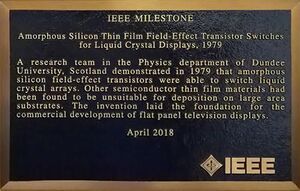
Milestones:Amorphous Silicon Thin Film Field-Effect Transistor Switches for Liquid Crystal Displays, 1979
- Date Dedicated
- 2018/04/05
- Dedication #
- 187
- Location
- Dundee, Scotland, UK
- IEEE Regions
- 8
- IEEE sections
- United Kingdom and Ireland
- Achievement date range
- 1979
Title
Amorphous Silicon Thin Film Field-Effect Transistor Switches for Liquid Crystal Displays, 1979
Citation
A research team in the Physics department of Dundee University, Scotland demonstrated in 1979 that amorphous silicon field-effect transistors were able to switch liquid crystal arrays. Other semiconductor thin film materials had been found to be unsuitable for deposition on large area substrates. The invention laid the foundation for the commercial development of flat panel television displays.
Street address(es) and GPS coordinates of the Milestone Plaque Sites
Physics Department, Dundee University, Dundee, Scotland, UK, 56.4582447, -2.9821428
Details of the physical location of the plaque
The plaque is mounted on the outside wall of the building.
How the plaque site is protected/secured
Dundee University campus security.
Historical significance of the work
The cathode ray tube (CRT) provided the principal means for displaying dynamic images from the 1930s until the advent of liquid crystal displays in the 1960s and 1970s. The standard level of definition for practical devices suitable for high data rate applications such as television, required that millions of pixels needed to be addressed for each frame to be displayed. This presented no special problem for electron beams scanned across a phosphor screen, but in a flat liquid crystal display direct electrical connection to each element was an essential requirement. At the selected pixel a switching voltage had to be supplied to turn on the local zone of the liquid crystal film for a very short time interval. This action allowed the back-lit light source to be viewed by the observer in front of the display. The complexity of connecting such a large and compact array of elements required a wiring matrix on a microscopic scale that could only be achieved by using a conducting film from which the circuitry could be fabricated. By using the film in the form of an amorphous silicon layer Spear and LeComber were able to design a series of switching transistors able to perform the necessary switching function at each pixel. Their breakthrough pointed the way for the manufacture of large flat panel displays.
Features that set this work apart from similar achievements
The concept of incorporating a switching device at each pixel of a flat panel display was first proposed by the RCA group of Weimer in 1961. It was not until a material able to be deposited over a large area suitable for a flat panel display became available that the invention could be used in a practical device. The semiconducting properties of thin layers or films are quite different from those of single crystal or polycrystalline versions. For example, conventional devices such as bipolar or field-effect transistors made from such films have generally poor performance. The Dundee group discovered that TFTs made from films of amorphous silicon to which hydrogen had been added (a-Si:H) could be used as effective switching devices.
Significant references
The most significant references are provided with this submission, and are on file with the staff of the IEEE History Center.
The following references have been chosen in support of the Milestone application for the recognition of the work of the Dundee University, Scotland, to develop amorphous silicon switches for flat panel displays.
1. Peter LeComber and Walter Spear in 1979 conducted the first successful experiments that demonstrated the feasibility of using thin films of amorphous silicon in large area flat panel displays.
It is cited in references a, b, c, and d as the most significant advance in flat panel technology.
2. Paul Weimer had reported in 1962 that it was possible to produce transistor action in thin film field effect devices. His paper announced the arrival of this new type of transistor which eventually became the preferred choice of switching device for flat panel displays.
3. Peter Brody and his team at Westinghouse Research reported their work on a ‘state of the art’ liquid crystal display that demonstrated that, in principle, practical-size substrates could be employed using directly addressed discrete thin film silicon transistors.
4. Howard’s 1992 paper reviews the progress achieved with thin-film transistor/liquid crystal displays. He cites the work of LeComber and Spear with the comment that ‘the report of an amorphous silicon TFT by LeComber et al in 1979 must be considered a major milestone’.
5. The paper by Hilsum in 2016 points out that the use of amorphous silicon by LeComber and Spear was entirely novel and unexpected, and followed a long sequence of unsuccessful attempts by other groups to use deposited films of other materials for fabticating the switching matrix.
6. The paper by Depp and Howard in 1993 notes that the advantage of the approach adopted by LeComber and Spear was that was cheaper than the alternatives, and therefore more commercially viable, and that the processing was simpler.
7. The review paper by Kuo in 2013 also cites the LeComber and Spear work as providing ‘the breakthrough in the field’.
In summary, these references confirm that the progress achieved since the 1960s towards a flat panel display using liquid crystals was punctuated with many disappointments. The lack of success in trying to use conventional semiconductor technology continued until the Dundee University group showed that amorphous silicon offered a better solution.
Supporting materials
Supporting materials were provided with this submission. Because of copyright, they may not be posted here. However, copies are on file with the staff of the IEEE History Center.
