Milestones:The Floating Gate EEPROM, 1976 - 1978
- Date Dedicated
- 2012/08/20
- Dedication #
- 127
- Location
- Milpitas, California, USA
- IEEE Regions
- 6
- IEEE sections
- Santa Clara Valley
- Achievement date range
- 1976-1978
Citation
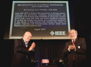
From 1976-1978, at Hughes Microelectronics in Newport Beach, California, the practicality, reliability, manufacturability and endurance of the Floating Gate EEPROM -- an electrically erasable device using a thin gate oxide and Fowler-Nordheim tunneling for writing and erasing -- was proven. As a significant foundation of data storage in flash memory, this fostered new classes of portable computing and communication devices which allow ubiquitous personal access to data.
Street address(es) and GPS coordinates
- Site 1: Western Digital (formerly SanDisk), 601 McCarthy Blvd., Milpitas, CA 95035 US (GPS: 37.417158, -121.920927).
- Site 2: Computer History Museum, 1401 N. Shoreline Blvd, Mountain View, CA 94043 US (GPS: 37.414757, -122.077679).
Details of the physical location of the plaque
- Site 1: In a small museum just off the Visitor's Lobby in Bldg. 6.
- Site 2: On the inside face of the front patio brick wall, near the Main Entrance.
How the intended plaque site is protected/secured
- Site 1: Normal weekday business hours.
- Site 2: Building security; 24/7 access.
Historical Significance
The plaque may be viewed at SanDisk Headquarters, 601 McCarthy Blvd., Milpitas, CA 95035 (37.417158,-121.920927). This is Bldg. 6, which includes the main Visitors' Lobby. The Visitors' Lobby has direct public access, and the building is locked during non-business hours.
EPROM, EEPROM, Flash EEPROM, NOR Flash and NAND Flash are non-volatile memory technologies that were introduced between 1970 and 1987.
While at Hughes Microelectronics, Eli Harari showed that thin SiO2 films (of about 100 Å) were an efficient and reliable electron conduction mechanism for both program and erase, and in fact allowed for the electrically-erasable floating gate EEPROM in 1976 (Ref. 3) as compared with the ultra-violet-erasable floating gate EPROM of 1970. The importance of this discovery continues to this day with thin SiO2 film being an essential characteristic of both NOR Flash and NAND Flash.
Eli’s 1977 JAP paper (Ref. 2, published in 1978) showed that the 1976 EEPROM was reliable, manufacturable, highly efficient and had high durability.
Eli’s EEPROM invention used Fowler-Nordheim tunneling for both write and erase operations. NOR Flash adopted use of hot electron injection for Write operations, but NAND Flash’s use of low current Fowler-Nordheim tunneling proved to be five to six orders of magnitude more efficient than NOR Flash. While NAND was initially considered a niche product since its serial access was considered inferior to NOR’s random access, this serial characteristic gives NAND a block storage property like that of a disk drive. NAND is thus more easily usable for data storage, and it also provides a denser and more scalable medium than NOR Flash.
The historic significance of the (1) thin film and (2) Fowler-Nordheim tunneling usage discoveries in 1976 and 1977 can be summarized as follows:
- All NAND Flash and a segment of the NOR Flash market relies on the thinness of SiO2 films (at about 100 Å) to enable its electron conduction for long-term retention of electrons trapped on a floating gate in a transistor.
- In concert with thin SiO2 films, NAND Flash’s reliance on the high efficiency provided by Fowler-Nordheim tunneling has allowed NAND to be optimized for the frequent Write/Erase operations of blocks of data as required for data storage usage.
Important Events in creating the Foundation for Data Storage in Flash Memory (1970-1987)
- 1969-73: Eli Harari researches areas including thin film SiO2 and tunneling phenomena while writing his Ph.D. thesis at Princeton University.
- 1970: Intel’s Dov Frohman-Bentchkowsky invents first ultra-violet-erasable floating gate EPROM, which used a thick gate oxide at a range of 1000 Å.
- 1973: Harari receives Princeton Ph.D. based on his study of thin film thermal oxide conduction and charge trapping mechanisms as detailed in his thesis Charge Trapping Effects in Thin Films of Al2O3 and SiO2 (Ref. 1).
- 1973-79: Harari is employed at Hughes Aircraft Company's Hughes Microelectronics Division at 500 Superior Ave., Newport Beach, CA.
- 1976-77: Harari invents the first practical Floating Gate EEPROM (US Pat. 4,115,914) (Ref. 3), an electrically-erasable floating gate device using a thin gate oxide at a range of 100 Å, and which included the use of Fowler-Nordheim tunneling for both write and erase operations. Importantly, the practicality of this Floating Gate EEPROM resulted from (1) the fact that this thin SiO2 was sufficiently thick (approx. 70-100 Å) to indefinitely store a floating gate charge for data storage, and (2) the use of polysilicon floating gates which were widely adopted in EPROM devices. [Note 1: the '914 patent has a priority date of 3/26/76, a filing date of 2/22/77 and an issue date of 9/26/78. The 1976-77 date of this entry is based on both the priority date and the filing date.] [Note 2: the '914 patent includes this reference on its cover page: "Tickle, et al.: Electrically Alterable Nonvolatile Semiconductor Memories, Session 4, 1972 Wescon Technical Papers." The Tickle device uses dual-gate MNOS devices (EAROM), and is thus not based on floating gates. Tickle's paper specifically relates to storage in a "gate insulating film having a charge storage function." Tickle's MNOS transistors in its Fig. 8a use two distinct gates, one for the variable threshold (Vt) write/erase and one for select only. This is in contrast to the '914 Fig. 8 embodiment which requires just a single gate. The Tickle device is an example of the many MNOS category devices that used direct tunneling from the silicon substrate to a layer of Silicon Nitride (which served as the trapping layer) through an utra-thin (approx. 25 Å) layer of SiO2, which proved insufficient for long-term data retention. The '914 patent’s use of Fowler-Nordheim tunneling onto a floating gate through thin (approx. 70-100 Å) SiO2 allowed long-term data retention to be realized. The Tickle device was referenced in the '914 patent not because of its write/erase mechanism (which was completely different from the '914 Fowler-Nordheim write/erase mechanism) but because its Fig. 8a teaches the integration of the select transistor with the variable threshold transistor, which is the case for some '914 embodiments such as Fig. 8 where the thin oxide rewritable region 56 is integrated with a fixed threshold selection transistor whose channel region 48 is integrated with 56.] [The Tickle paper is available here: http://www.bswd.com/TicklePaper-Wescon1972.pdf]
- 1977-78: Harari wrote the Journal of Applied Physics (JAP) paper Dielectric breakdown in electrically stressed thin films of thermal SiO2 (Ref. 2, written in 1977 and published in 1978) which explained the physics of conduction, trapping and eventual breakdown of thin SiO2 films in the range of 45 Å to 160 Å operating under high electric field conditions. Under such conditions these films exhibited highly efficient tunneling current through the SiO2 insulator, and this Fowler-Nordheim tunnel conduction mechanism became the foundation for write/erase operations in EEPROM, and later in Flash EEPROM. This seminal work also showed that thin SiO2 films were reliable, manufacturable and highly efficient for numerous write/erase cycles. Harari further described the basic tools and techniques for characterizing and optimizing such films (e.g., Tbd-time to breakdown and Qbd-trapped charge at breakdown) which paved the way for their incorporation first into EEPROM, then into Flash EEPROM, and eventually and in particular into NAND Flash.
- 1978: Harari and three others from Hughes Microelectronics present a paper titled A 256-Bit Nonvolatile Static RAM at the IEEE ISSCC Conference in February 1978 (Ref. 8). Fig. 4 of this paper shows a cross-section of the EEPROM cell, which corresponds to the EEPROM embodiment of Fig. 6 in the '914 patent (Ref. 3). This paper highlights in substantial detail the role of the area of thin SiO2 for tunnel program/erase of the state of the static RAM cell, and clearly emphasizes the ~90% strong capacitive coupling of the Floating Gate to the control gate that makes this cell work properly. This operation is in contrast with the low capacitive coupling described in the Kahng/Sze 1967 paper titled "A floating gate and its application to memory devices," a characteristic which made the Kahng/Sze cell impractical. Note that the device described in Ref. 8 is 256-bit nonvolatile SRAM, i.e., an SRAM that is backed up by EEPROM so as to retain its data when power is lost.
- 1979-81: Harari joins Intel and serves as Manager of Intel's Santa Clara Technology Development Group, which is focused on non-volatile memory, and in particular EPROM and EEPROM.
- 1980-82: Intel, Seeq and Hughes Microelectronics successfully commercialize Harari’s EEPROM invention, based on the technology described in Refs. 2 and 3. The Intel 2816 was a 16K bit HMOS EEPROM, and the Hughes 3108 was an 8K bit CMOS EEPROM.
- 1984: Toshiba’s Fujio Masuoka invents Flash EEPROM, but it was a triple polysilicon device that employed thick SiO2, and thus used neither thin SiO2 nor Fowler-Nordheim tunneling. It was never successfully commercialized.
- 1984-87: Exel and Intel each separately invent NOR Flash, based on thin SiO2, but also hot electron injection instead of Fowler-Nordheim tunneling for Write/Erase operations. Intel successfully commercialized NOR Flash in 1987 under its ETOX trademark, and it was quickly adopted as the industry standard Flash because it was plug-and-play compatible with Intel's EPROM. ETOX was designed primarily for code-store applications, where write and erase were infrequent.
- 1987: Toshiba’s Fujio Masuoka invents NAND Flash, an EEPROM device based on thin SiO2 (about 100 Å), and Fowler-Nordheim tunneling for Write/Erase operations. This invention thus embraced the Write/Erase mechanism described in both Harari’s 1976 EEPROM invention and Harari's 1978 JAP paper.
Subsequent Events that led to Tremendous Growth in the Data Storage in Flash Memory Industry (1988-present)
The above foundation led to Harari recognizing that Data-Store applications were far less forgiving than Code-Store. Data-Store applications were totally intolerant of any error-bits occurring during multiple write/erase cycles or after long-term data retention. Unlike other memories such as SRAM and DRAM, random Flash cells would begin to wear out and eventually break down or lose their stored charge during years of field operation.
If very large Flash memory arrays containing billions of Flash EEPROM transistors were to meet zero bit-error reliability levels, it was not sufficient to apply error correcting code (ECC) and spare/redundant rows and columns blown in the factory, the techniques commonly employed in 1988. Harari reasoned that what was required was a holistic "System Flash" solution that would accompany the Flash EEPROM through its entire lifetime.
Harari proposed a radically new block-oriented Flash memory array architecture, working cooperatively with a sophisticated intelligent controller. This architecture would manage, detect, and correct or replace any and all defective cells, either before failures occurred or as soon as such failures were detected. What resulted was the invention of SanDisk's System Flash. This was an approach that was later adopted by the entire Flash Data-Store industry, including virtually all of today's Flash cards, USB Flash drives, embedded Flash, managed NAND and SSDs.
The inventions that incorporated the System Flash architecture were:
- 1988: Harari invents multistate flash with adaptive program and erase cycles "making it particularly useful as a solid state memory in place of magnetic disk storage devices" (US Pat. 5,095,344) (Ref. 4)
- 1989: Harari and SunDisk colleagues invent massively parallel multistate flash programming, and program-inhibit for verified cells (US Pat. 5,172,338) (Ref. 5) [Note: SunDisk Corp. became SanDisk Corp. in August 1995.]
- 1989: Harari and SunDisk colleagues invent "System Flash," a radical new concept in which a "system of Flash EEprom memory chips with controlling circuits serves as non-volatile memory such as that provided by magnetic disk drives" by coupling a controller, firmware and flash cells to manage program/erase operations and to remap/replace defective cells with substitute cells (US Pat. 5,297,148) (Ref. 6)
While NOR Flash adopted use of a thin SiO2 gate dielectric, its use of hot electron injection for Write operations proved to be five to six orders of magnitude less efficient than Fowler-Nordheim tunneling. This choice was dictated for NOR Flash somewhat because it sought compatibility with EPROM, whose random access was optimized for storing micro-code since it rarely required multiple Write/Erase cycles. NOR Flash was an easy design-in for EPROM and gained early success in the market.
By contrast, the high efficiency provided by Fowler-Nordheim tunneling allowed NAND Flash to be optimized for data storage, a usage that required multiple frequent Write/Erase operations of blocks of data. The enablement of hard disk emulation by way of the “System Flash” invention (Ref. 6) allowed NAND Flash to begin to displace hard disk storage, and to allow for data storage in very small low-power devices. Harari’s multistate flash invention (Refs. 4 and 5) allowed for large price savings and greater density, thereby speeding the adoption of NAND Flash.
NAND Flash's adoption of Fowler-Nordheim tunneling gave it the winning hand in overtaking NOR Flash and thereby dominating the Flash market since early in the current millennium. NAND Flash is now ubiquitous around the world, having enabled portable electronics in numerous areas including digital photography, digital music, smart phones and tablet computing.
Eli was the 2009 IEEE Robert N. Noyce Medal Recipient, as noted here:
http://www.ieee.org/about/awards/bios/noyce_recipients.html#sect3
Features or characteristics which set this work apart from similar achievements
The Foundation of Flash Memory -- By exploring much thinner SiO2 films in the 100 Å range at Hughes, Eli Harari showed that, under high electric field conditions, electron conduction through these films was an efficient and reliable mechanism for both program and erase. This change from the 700-1000 Å thickness used in the 1970 ultra-violet-erasable floating gate EPROM was critical to the success of the 1976 electrically-erasable floating gate EEPROM. The importance of this discovery continues to this day with this thin SiO2 film having always been an essential characteristic of both NOR Flash and NAND Flash.
Harari also showed that the phenomenon responsible for the efficiency and reliability of these much thinner SiO2 films was indirect tunneling from the silicon conduction band to the SiO2 conduction band, a quantum mechanical effect known as Fowler-Nordheim tunneling which was first discovered by Fowler and Nordheim many years earlier. This mode of conduction was important because 100 Å films of SiO2 would support long-term retention of electrons trapped on a floating gate. This is in sharp contrast to the 25-30 Å films of SiO2 that were employed in earlier days in MNOS/SONOS for direct tunneling of electrons from the silicon conduction band into interface traps, and which were generally unreliable and incapable of long-term retention of trapped electrons. The importance of Fowler-Nordheim tunneling has been fundamental to the success of NAND Flash, as compared with the use of hot electron injection in the far less popular NOR Flash.
Thus, thin SiO2 films were a fundamental enabler of both NOR and NAND Flash, and Fowler-Nordheim tunneling was a fundamental enabler of NAND Flash.
The Evolution of Flash Memory -- In 1989, “System Flash” overcame the unreliable nature of flash memory with a technique that created a long-term non-volatile medium that could be reliably rewritten, and which included the ability to remap and replace defective and “worn out” cells with substitute cells.
While NAND was initially considered a niche product since its serial access was considered inferior to NOR’s random access, this serial characteristic gave NAND a block storage property like that of a disk drive. This resulted in SanDisk's controversial decision to transition from NOR to NAND in the late 1990s, a move that resulted in lower cost, scalability, and the ability to support massive parallelisms in program (write) and erase operations. Cost reductions were accelerated through the successful commercialization of 2 bits-per-cell (X2) and 3 bits-per-cell (X3) multistate NAND technology.
The ability of products implementing “System Flash” to emulate random access disk sectors allowed them to be a direct replacement for magnetic storage. Their compact size and low-power filled a niche that could not be filled by disk drives, and high volumes have allowed advances in NAND flash memory to outpace Moore’s Law.
References, citations, and supporting material
IEEE-MilestoneProposal-DataInFlashMemory-Background2.pdf
Ref. 1: Abstract of Eli Harari's Princeton Ph.D. Thesis (1973)
Ref. 2: Harari Journal of Applied Physics (JAP) Paper (1978; submitted in 1977)
Ref. 7: Harari IEEE Int'l. Memory Workshop (IMW) Presentation (2011)
Ref. 8: ISSCC Paper Disclosing Device Based on '914 Patent (1978)
Ref. 9: Eli Harari Oral History
Dedication Ceremony
Map
